
 대표어
대표어


권호기사보기
| 기사명 | 저자명 | 페이지 | 원문 | 기사목차 |
|---|
결과 내 검색
동의어 포함
Title Page
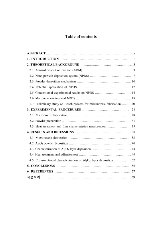
Contents
ABSTRACT 5
1. INTRODUCTION 6
2. THEORETICAL BACKGROUND 8
2.1. Aerosol deposition method (ADM) 8
2.2. Nano particle deposition system (NPDS) 12
2.3. Powder deposition mechanism 15
2.4. Potential application of NPDS. 17
2.5. Conventional experimental results of NPDS 19
2.6. Micronozzle-integrated NPDS 23
2.7. Preliminary study on Bosch process for micronozzle fabrication 25
3. EXPERIMENTAL PROCEDURES 33
3.1. Micronozzle fabrication 33
3.2. Powder preparation 36
3.3. Heat treatment and film characteristics measurement 40
4. RESULTS AND DISCUSSIONS 43
4.1. Micronozzle fabrication 43
4.2. Al₂O₃ powder deposition 45
4.3. Characterization of Al₂O₃ layer deposition 49
4.4. Heat treatment and adhesion test 54
4.5. Cross-sectional characterization of Al₂O₃ layer deposition 57
5. CONCLUSIONS 61
6. REFERENCES 62
국문 요지 64
감사의 글 65
Fig. 2.1: Configuration of the aerosol deposition equipment. 10
Fig. 2.2: Illustration of Al₂O₃ film formation mechanism in the aerosol deposition method in the case of (a) room temperature conditions, and (b) higher temperatures [16] : (1) particle; (2) substrate; (3) particle deposited before. The time line is given. 11
Fig. 2.3: Particle velocity and diameter range of various powder deposition methods. 13
Fig. 2.4: Schematics of NPDS [11]. 14
Fig. 2.5: Micropatterning principle of NPDS. 16
Fig. 2.6: Potential application of NPDS. 18
Fig. 2.7: TiO₂ nanopowder deposition on AlSI304 stainless steel. (a) Surface image taken by scanning electronic microscope (SEM). (b) The cross-sectional image taken by SEM. 20
Fig. 2.8: (a) The SEM image of Al₂O₃ powders (before deposition). (b) The SEM image of the surface of deposited Al₂O₃ area (after deposition). 22
Fig. 2.9: Fabrication of micronozzles using semiconductor technologies [17, 18, 19]. 24
Fig. 2.10: SEM images of the cross-sectional area of Si trenches as the duty cycle and width change. 28
Fig. 2.11: Relation between the etch rate and duty cycle with changes in nominal width. 29
Fig. 2.12: Relationship between the etch rate and aspect ratio of trenches with various duty cycles. 30
Fig. 2.13: Relationship between the duty cycle and undercut as the nominal width changes. 31
Fig. 2.14: Relationship between the bowing effect and duty cycle as the nominal width changes. 32
Fig. 3.1: Micronozzle fabrication process flow chart. nozzle: (a) Wafer preparation; (b) Photoresist patterning; (c); (c) Isotropic etching; (d) Deep reactive ion etching; (e) Photoresist stripping; (f) Back-side alignment and Photoresist patterning; (g) Isotropic etching; (h) Deep reactive ion etching; (i) Stripping of photoresist and... 34
Fig. 3.1: SEM image of a-Al₂O₃ powder. 38
Fig. 3.2: X-ray diffraction pattern Al₂O₃ powder. The peak indicates that the type is a- Al₂O₃ (the reference peak of a-Al₂O₃ is shown below the measured peak). 39
Fig. 3.2: Annealing temperature profile. 41
Fig. 4.1: Optical image of micronozzle: (a) Schematic showing the difference between the original pattern and the actual etching of the nozzle. (b) Optical image of the fabricated micro-nozzle. (c) Schematic of cross-sectional view for micronozzle across A-A' line in the optical image. 44
Fig. 4.2: Optical images of heat-treated Al₂O₃ layers deposited on various substrates: (a) Si substrate with 0 s ultrasonic treatment; (b) Si substrate with 2 s ultrasonic treatment; (c) Si substrate with 7 s ultrasonic treatment; (d) Al substrate with 0 s ultrasonic treatment; (e) Al substrate with 2 s ultrasonic treatment; (f) Al substrate... 47
Fig. 4.3: Fluid behavior at the nozzle tip [21]. The carrier moves directly towards the substrate when the Stokes number is greater than 1. 48
Fig. 4.4: Image of Al₂O₃ powder deposition on Cu substrate observed by SEM. (a) Overall image. (b) Al₂O₃ powder deposition layer (the investigated area is designated in (a)) Powders were densely deposited. (c) Highly magnified Al₂O₃ powder image showing that the deposited Al₂O₃ layer is melted (the investigated... 51
Fig. 4.5: Image of Al₂O₃ powder deposition on Al substrate observed by SEM. (a) Overall image. (b) Al₂O₃ powder deposition layer (the investigated area is designated in (a)). Powders were densely deposited. (c) Highly magnified Al₂O₃ powder image (the investigated area is designated in (b)). (d) Highly magnified... 52
Fig. 4.6: Image of Al₂O₃ powder deposition on Si substrate observed by SEM. (a) Overall image. (b) Al₂O₃ powder deposition layer (the investigated area is designated in (a)). (c) Highly magnified Al₂O₃ powder image (the investigated area is designated in (a)). (e) Highly magnified melted Al₂O₃ powder image (the investigated... 53
Fig. 4.7: The thickness of remaining Al₂O₃ powders on various substrates after different ultrasonic treatments. 56
Fig. 4.8: (a) Cross-sectional view of the Al₂O₃ powder pattern deposited on the Cu substrate. EDX analysis position was designated on the image. (b) Al peak detection result on the designated line. (c) Cu peak detection result on the designated line. (d) Oxygen peak detection result on the dotted line. (e) Highly magnified cross-sectional... 58
Fig. 4.9: (a) Cross-sectional view of the Al₂O₃ powder pattern deposited on the Al substrate. EDX analysis position was designated on the image. (b) Al peak detection result on the dotted line. (c) Oxygen peak detection result on the designated line. (d) Highly magnified cross-sectional image. The magnified location is indicated in (a). 59
Fig. 4.10: (a) Cross-sectional view of the Al₂O₃ powder pattern deposited on the Cu substrate. EDX analysis position was designated on the image. (b) Al peak detection result on the designated line. (c) Si peak detection result on the designated line. (d) Oxygen peak detection result on the dotted line. (e) Highly magnified cross-sectional... 60
*표시는 필수 입력사항입니다.
| 전화번호 |
|---|
| 기사명 | 저자명 | 페이지 | 원문 | 기사목차 |
|---|
| 번호 | 발행일자 | 권호명 | 제본정보 | 자료실 | 원문 | 신청 페이지 |
|---|
도서위치안내: / 서가번호:

우편복사 목록담기를 완료하였습니다.
*표시는 필수 입력사항입니다.
저장 되었습니다.
