

권호기사보기
| 기사명 | 저자명 | 페이지 | 원문 | 기사목차 |
|---|
| 대표형(전거형, Authority) | 생물정보 | 이형(異形, Variant) | 소속 | 직위 | 직업 | 활동분야 | 주기 | 서지 | |
|---|---|---|---|---|---|---|---|---|---|
| 연구/단체명을 입력해주세요. | |||||||||
|
|
|
|
|
|
* 주제를 선택하시면 검색 상세로 이동합니다.
Title Page
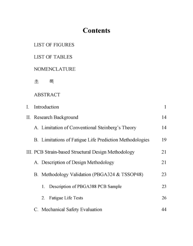
Contents
NOMENCLATURE 13
초록 16
ABSTRACT 20
I. Introduction 23
II. Research Background 36
A. Limitation of Conventional Steinberg's Theory 36
B. Limitations of Fatigue Life Prediction Methodologies 41
III. PCB Strain-based Structural Design Methodology 43
A. Description of Design Methodology 43
B. Methodology Validation (PBGA324 & TSSOP48) 45
1. Description of PBGA388 PCB Sample 45
2. Fatigue Life Tests 48
C. Mechanical Safety Evaluation 66
D. Methodology Validation (PBGA388 Package) 85
1. Description of PBGA388 PCB Sample 86
2. Fatigue Life Tests 91
3. Mechanical Safety Evaluation 102
IV. PCB Strain-based Structural Design Methodology for Rapid Evaluation of Spacebome Electronics 119
A. Description of Design Methodology 121
1. FEM Construction & Modal Analysis (Step 1-2) 125
2. Estimation of TTFreq for Survival in Vibration Test and Launch Process (Step 3-4)[이미지참조] 126
3. DF Estimation & MoS Calculation with respect to PCB Strain (Step 5-6) 130
B. Fatigue Life Tests 131
1. Description of PBGA388 PCB Sample (Sample Set #1) 131
2. Results of Fatigue Life Tests 135
C. Methodology Validation 140
1. FEM Modeling Technique of PCB 142
2. Mechanical Safety Evaluation 147
D. Methodology Validation on Various Packages 167
1. Sample Set #2: CCGA624 Package 167
2. Sample Set #3: QFP208 Package 169
3. Sample Set #4: PBGA388 Package 179
E. Considerations in Practical Structural Design of Spaceborne Electronics 183
V. Conclusion 195
VI. Future Study 199
References 201
Research Achievements 208
Fig. I-1. Various types of integrated electronic packages 31
Fig. I-2. Typical launch and ascent process of launcher 32
Fig. I-3. Conventional fatigue life prediction approach for solder joint under vibration 33
Fig. I-4. Fatigue life prediction approach using Sherlock tool 34
Fig. I-5. Number of small satellite development in 2000-2020 35
Fig. II-1. Geometrical factors for Steinberg's empirical formula (Eq. (II-1)) 37
Fig. II-2. Example of complex mode shapes of PCB 39
Fig. II-3. Example of PCB with irregular fixation points, making ambiguous to determine... 40
Fig. III-1. Configuration of PCB sample with PBGA packages and TSSOPs 46
Fig. III-2. Representative X-ray inspection results on U5 BGA solder joints 51
Fig. III-3. Representative optical inspection results on U3 TSSOP solder joints 52
Fig. III-4. Random vibration fatigue test set-up 53
Fig. III-5. Configuration of daisy-chain circuit for PBGA324 package 55
Fig. III-6. Configuration of daisy-chain circuit for TSSOP48 56
Fig. III-7. Time profiles of daisy-chain resistance on each packages of PBGA324 &... 57
Fig. III-8. Time profiles of daisy-chain resistance on each packages of PBGA324 &... 58
Fig. III-9. SEM micrographs on solder joint of U2 package of PCB sample #2 59
Fig. III-10. SEM micrographs on solder joint of U1 package of PCB sample #2 60
Fig. III-11. SEM micrographs on solder joint of U4 package of PCB sample #2 61
Fig. III-12. SEM micrographs on solder joint of U5 package of PCB sample #2 62
Fig. III-13. SEM micrographs on solder joint of U6 package of PCB sample #2 63
Fig. III-14. SEM micrographs on solder joint of U9 package of PCB sample #2 64
Fig. III-15. Evaluation scheme for structural design methodology (w.r.t PBGA324 &... 71
Fig. III-16. Configuration of detailed FEM of PBGA324 & TSSOP48 PCB sample 72
Fig. III-17. Representative mode shapes of PCB sample 75
Fig. III-18. Configuration of simplified FEM of PBGA324 & TSSOP48 PCB sample 78
Fig. III-19. Random vibration fatigue test set-up of PCB sample with CCGA package 81
Fig. III-20. Time profile of daisy-chain resistance of CCGA package 82
Fig. III-21. Representative optical micrograph of CCGA solder joints 83
Fig. III-22. Case 1 PCB sample with PBGA388 package 87
Fig. III-23. Configurations of PCB samples in each case (Cases 1, 1-1 and 1-2) 89
Fig. III-24. Configurations of PCB samples in each case (Cases 1, 2 and 3) 90
Fig. III-25. Fatigue life test set-up for PBGA388 PCB samples 93
Fig. III-26. Configuration of daisy-chain circuit for PBGA388 package 94
Fig. III-27. Time profiles of daisy-chain resistance on each PBGA388 PCB samples 96
Fig. III-28. SEM microphotograph of cracked BGA solder joints of Case 1 sample 97
Fig. III-29. SEM microphotograph of cracked BGA solder joints of Case 1-1 sample 98
Fig. III-30. SEM microphotograph of cracked BGA solder joints of Case 2 sample 99
Fig. III-31. SEM microphotograph of cracked BGA solder joints of Case 3 sample 100
Fig. III-32. Configuration of (a) detailed and (b) simplified FEMs of Case 1 sample 105
Fig. III-33. Mode shapes of Case 1 PCB ((a) 213.5 Hz, (b) 408.1 Hz, (c) 538.7 Hz) 108
Fig. III-34. Von-mises stress distributions of Case 1 PCB sample 110
Fig. III-35. Von-mises stress distributions of Case 1-2 PCB sample 111
Fig. III-36. Summary of fatigue life prediction results on solder joints of PCB samples 113
Fig. III-37. Evaluation scheme for structural design methodologies (w.r.t PBGA388 packages) 116
Fig. IV-1. Evaluation approach on structural design of spaceborne electronics using Oh-... 124
Fig. IV-2. Assumed scenario of test and launch processes for spaceborne electronics 129
Fig. IV-3. Representative configuration of sample PCB assembly in Case 1 133
Fig. IV-4. Configuration of daisy-chain circuit for PBGA388 package 134
Fig. IV-5. Fatigue life test set-up for a set of PCB samples 136
Fig. IV-6. Time profile of measured daisy-chain resistance for each sample during... 138
Fig. IV-7. Validation scheme for Oh-Park methodology 141
Fig. IV-8. Example of FEM of PCB assembly with Case 1 modeling technique for... 144
Fig. IV-9. Various simplified modeling techniques for electronic package ((a) Type 1 (4... 145
Fig. IV-10. Calculation method to derive εpmax from simplified FEM[이미지참조] 146
Fig. IV-11. Measured and analyzed PSD acceleration responses of bare PCB in Case 1... 149
Fig. IV-12. Measured and analyzed PSD acceleration responses of bare PCB in Case 2... 150
Fig. IV-13. Measured and analyzed PSD acceleration responses of bare PCB in Case 3... 151
Fig. IV-14. Mode shapes of sample PCB in Case 1 with Type 3 package modeling ((a) 1st... 154
Fig. IV-15. Estimated DF for estimated TTFreq as a function of fn[이미지참조] 157
Fig. IV-16. Comparison between TTFtest and TTFpred calculated by methodologies...[이미지참조] 162
Fig. IV-17. Comparison between TTFtest and TTFpred calculated by methodologies...[이미지참조] 164
Fig. IV-18. Comparison between TTFtest and TTFpred calculated by methodologies...[이미지참조] 166
Fig. IV-19. Illustration of PCB sample with QFP208 package 171
Fig. IV-20. Random vibration test set-up for QFP208 PCB sample (sample set #3) 173
Fig. IV-21. Time profile of daisy-chain resistance for QFP208 package (sample set #3) 174
Fig. IV-22. Simplified FEM modeling technique for QFP package 175
Fig. IV-23. Representative mode shapes of QFP208 PCB ((a) 119.0 Hz, (b) 216.1. Hz, (c) 374.1 Hz) 177
Fig. IV-24. Illustration of PCB sample with PBG388 package 180
Fig. IV-25. Time profile of daisy-chain resistance for PBGA388 package (sample set #4) 181
Fig. IV-26. Assumed electronics development scenario 1 (Typical QM-FM approach) 189
Fig. IV-27. Assumed electronics development scenario 2 (PFM approach) 191
Fig. IV-28. Assumed electronics development scenario 3 (for reusable launch vehicle) 193
*표시는 필수 입력사항입니다.
| *전화번호 | ※ '-' 없이 휴대폰번호를 입력하세요 |
|---|
| 기사명 | 저자명 | 페이지 | 원문 | 기사목차 |
|---|
| 번호 | 발행일자 | 권호명 | 제본정보 | 자료실 | 원문 | 신청 페이지 |
|---|
도서위치안내: / 서가번호:

우편복사 목록담기를 완료하였습니다.
*표시는 필수 입력사항입니다.
저장 되었습니다.
