


권호기사보기
| 기사명 | 저자명 | 페이지 | 원문 | 기사목차 |
|---|
| 대표형(전거형, Authority) | 생물정보 | 이형(異形, Variant) | 소속 | 직위 | 직업 | 활동분야 | 주기 | 서지 | |
|---|---|---|---|---|---|---|---|---|---|
| 연구/단체명을 입력해주세요. | |||||||||
|
|
|
|
|
|
* 주제를 선택하시면 검색 상세로 이동합니다.
Title Page
Abstract
Contents
Chapter 1. Introduction 15
1.1. Motivation 15
1.2. Research scope and overview 17
Research thrust 1. A material perspective approach to investigate the significance of the combined use of LM and NW. 18
Research thrust 2. A process perspective approach to explore the relationship between laser and the mixture of LM and NW 19
1.3. Dissertation layout 21
Chapter 2. Literature Review 22
2.1. Stretchable electronics from a material perspective 22
2.1.1. Bulk liquid metal 22
2.1.2. Liquid metal particle and composite 25
2.1.3. Metallic nanowire 27
2.2. A study on a laser from a process perspective 28
2.2.1. Classification according to the laser pulse length 28
2.2.2. Laser-derived effects and applications 29
Chapter 3. Fundamental Study on Material and Laser Process 31
3.1. Liquid metal 31
3.1.1. From bulk liquid metal to liquid metal particle 31
3.1.2. Development of laser based liquid metal patterning framework 34
3.2. Introduction of additional material to EGaInPs 39
3.2.1. Copper plate and copper nanowire 39
3.2.2. Silver nanowire 40
Chapter 4. Fabrication of Uniform Liquid Metal Film 48
4.1. Necessity of uniform film for laser processing 48
4.2. Introduction of vacuum filtration technique 51
4.3. An effort to increase the yield of the liquid metal film 55
4.3.1. EGaIn particle size 55
4.3.2. Amount of AgNW 55
4.3.3. Comparison with other mixtures 57
Chapter 5. Percolation Network Simulation 62
5.1. Percolation theory and Monte Carlo simulation 62
5.2. Simulation for defect-free film formation condition 63
5.2.1. Numerical modeling for nanowires 63
5.2.2. Consideration of EGaIn particle 64
5.2.3. Verification and validation of simulation with experiment result 66
Chapter 6. Laser-Induced Biphasic Metallic Composite 73
6.1. Entanglement phenomenon 73
6.2. Theoretical approach 78
6.2.1. Wettability 78
6.2.2. Plasmonic effect 80
6.3. The degree of entanglement between EGaIn and AgNW 83
6.3.1. A quantitative analysis 83
6.3.2. Analysis of etching 84
6.3.3. Assessment of electromechanical behavior 87
6.4. Utilization of LIBMC 101
6.4.1. Necessity of the LIBMC heater 101
6.4.2. Demonstration of prototype 102
Chapter 7. Conclusions 110
7.1. Contributions and significance 110
7.2. Suggestions for future research 113
References 115
국문 초록 130
Figure 1-1. Keywords and scope of the dissertation 20
Figure 3-1. Synthesized EGaIn (eutectic gallium-indium alloy). 35
Figure 3-2. Fabricated EGaInP solution using the stirring method (left) and an optically magnified image of the solution (right). 35
Figure 3-3. EGaInP solution (left) and thin film from the solution (right) 36
Figure 3-4. Fabrication of EGaInPs using a tip sonicator. 36
Figure 3-5. EGaInP solution fabricated using the tip sonication method. 37
Figure 3-6. Schematic illustration of EGaIn patterning framework. 37
Figure 3-7. EGaIn patterns on the PDMS substrate. 38
Figure 3-8. EGaIn coating on copper foil 43
Figure 3-9. No reaction between EGaIn and CuNW film 43
Figure 3-10. Schematic illustration of patterning process on the CuNW film 44
Figure 3-11. The square-shape EGaIn pattern on the CuNW film 44
Figure 3-12. SEM image of transferred EGaInPs with CuNW 45
Figure 3-13. Comparison of (i)CuNW and (ii)AgNW with EGaInPs 45
Figure 3-14. Sheet resistance according to the amount of AgNW and EGaIn 46
Figure 3-15. Before(a) and after(b) laser irradiation to AgNW-EGaInPs mixture 47
Figure 3-16. Schematic illustration of stretchable conductor fabrication process 47
Figure 4-1. EGaInPs film from (a) drop casting method and (b) spin coating method 50
Figure 4-2. Schematic illustration of vacuum filtration and transfer (VFT) method. 53
Figure 4-3. Comparison of VFT results for (i)EGaInPs only and (ii) AgNWs-EGaInPs mixture 53
Figure 4-4. Thickness of the transferred AgNW-EGaInPs film. 54
Figure 4-5. Quality of the transferred EGaInPs film as the average particle size (dp).[이미지참조] 60
Figure 4-6. Difference of lump debris according to the amount of AgNW. 60
Figure 4-7. Sheet resistance data as the amount of AgNW increases 61
Figure 4-8. Transferred films through VFT technique on the various substances. 61
Figure 5-1. Schematic illustration of a single NW with the coordinate system 68
Figure 5-2. Scattered NWs in the window 68
Figure 5-3. NWs (black) and effective NWs (blue) 69
Figure 5-4. Definition of the intertwining scope (red circle) 69
Figure 5-5. Simulation results based on the number of NWs (100, 200, 500, 1000, 2000, and 4000 EA) 70
Figure 5-6. A binary plot of extracted intertwining scope based on the number of NWs (100, 200, 500, 1000, 2000, and 4000 EA) 71
Figure 5-7. 5000 NWs covered 88.9 % of the unit area. 72
Figure 6-1. Schematic illustration of principle of the LIBMC formation. 76
Figure 6-2. Visualization of calculated energy density. 76
Figure 6-3. Parametric study results based on the laser power and scanning speed. 77
Figure 6-4. Schematic representation of the AgNW-EGaInPs 81
Figure 6-5. Result of FDTD simulation at AgNW junction 81
Figure 6-6. AgNW-EGaInPs film in high temperature environment. 82
Figure 6-7. Laser irradiation to the mixture of bulk EGaIn and AgNWs 91
Figure 6-8. Laser irradiation to the mixture of EGaInPs and AgNWs 91
Figure 6-9. SEM and EDS for Ga and Ag components in the LIBMC 92
Figure 6-10. Relative comparison of XRD data 92
Figure 6-11. XRD results of the LIBMC (top) and AgNW-EGaIn film (bottom) 93
Figure 6-12. Etching result of LIBMC with SEM images based on the laser intensity. 94
Figure 6-13. LIBMC electrode before and after etching process. 94
Figure 6-14. Schematic illustration of the selective laser patterning and etching in the AgNWs-EGaInPs film. 95
Figure 6-15. SEM images for (i) the LM anchoring and (ii) the LM stacking 95
Figure 6-16. LIBMC conductor: (i) computer-aided drawing, (ii) prototype, and (iii) grid. 96
Figure 6-17. Direct laser pattering on various substrates. 96
Figure 6-18. Schematic illustration of the laser system 97
Figure 6-19. Characteristic profile for Gaussian (left) and flat-top beam (right) 97
Figure 6-20. Sheet resistance measurement as a function of laser power before (red) and after (blue) etching. 98
Figure 6-21. Relative change in resistance as a function of uniaxial tensile strain on PDMS before etching with various laser conditions. 98
Figure 6-22. Relative change in resistance as a function of uniaxial tensile strain on PDMS after etching with various laser conditions. 99
Figure 6-23. Cyclic test data for the LIBMC conductor. 99
Figure 6-24. Performance assessment by types of the stretchable electrode 100
Figure 6-25. Example of industrial application as electric heater 105
Figure 6-26. Differences of heating wire resistivity by zone 105
Figure 6-27. Conceptual image of LIBMC heater by applying varying conductivity characteristics 106
Figure 6-28. LIBMC heater design and fabricated prototype 106
Figure 6-29. Transient average temperature evolution of the LIBMC heater under zero strain at stepwise voltage rise from 0 to 4 V 107
Figure 6-30. Average temperature for the regions at a constant applied voltage of 4 V under strain variation 108
Figure 7-1. Schematic illustration of crucial points of the LIBMC conductor 112
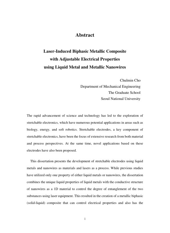
근래들어 광범위한 과학 기술의 발전 덕분에 바이오, 에너지, 소프트 로봇 등 다양한 어플리케이션에 광범위하게 활용 가능한 스트레쳐블 일렉트로닉스가 활발히 연구되고 있다. 스트레쳐블 일렉트로닉스의 근간이 되는 스트레쳐블 전극은 다양한 소재 및 공정적 관점에서 집중적으로 연구가 되는 한편, 이를 기반한 인간 삶에 도움이 될 수 있는 새로운 어플리케이션들 또한 계속 보고되고 있다. 본 학위논문에서는 재료적 관점에서 액체 금속과 나노 와이어를, 그리고 공정적 관점에서 레이저를 선정하여 스트레쳐블 전극을 개발한 것을 보고한다. 기존 연구들이 액체 금속과 나노 와이어의 한 속성만을 이용하였다면, 본 학위 논문에서는 액체 금속이 지니고 있는 특유의 액체적 성질과 나노 와이어의 1D 물질로서 전도성 구조체를 이룰 수 있는 성질을 조합하여, 레이저 장비를 통해 원하는 영역만 두 물질의 얽힘의 정도를 조절시켰다. 이로부터 전기적 물성이 조절 가능한 금속성 2상 (고체-액체) 복합체를 개발하여 히터로서 그 활용 가능성을 확인하였다. 한편, 균일한 성능을 가진 동일 전극을 제작하기 위하여 본 학위논문에서 새롭게 고안된 감압여과 방식 필름 제작 및 이에 관련된 시뮬레이션 연구는 향후 다른 연구자들에게 본 연구에 근간한 새로운 연구를 위한 좋은 밑거름이 될 것이다.
*표시는 필수 입력사항입니다.
| *전화번호 | ※ '-' 없이 휴대폰번호를 입력하세요 |
|---|
| 기사명 | 저자명 | 페이지 | 원문 | 기사목차 |
|---|
| 번호 | 발행일자 | 권호명 | 제본정보 | 자료실 | 원문 | 신청 페이지 |
|---|
도서위치안내: / 서가번호:

우편복사 목록담기를 완료하였습니다.
*표시는 필수 입력사항입니다.
저장 되었습니다.
