 학술연구정보서비스(KERIS)


권호기사보기
| 기사명 | 저자명 | 페이지 | 원문 | 기사목차 |
|---|
| 대표형(전거형, Authority) | 생물정보 | 이형(異形, Variant) | 소속 | 직위 | 직업 | 활동분야 | 주기 | 서지 | |
|---|---|---|---|---|---|---|---|---|---|
| 연구/단체명을 입력해주세요. | |||||||||
|
|
|
|
|
|
* 주제를 선택하시면 검색 상세로 이동합니다.
Title Page
Abstract
Contents
List of Abbreviations 16
Chapter 1. Introduction 18
1.1. Background 19
1.2. Spiking Neural Networks 23
1.3. Purpose of research 26
1.4. Thesis Structure 28
Chapter 2. Biological Neuron Model 29
2.1. Electrical input-output membrane voltage models 30
2.1.1. Perfect Integrate-and-fire 31
2.1.2. Hodgkin-Huxley Model 33
2.1.3. Adaptive Integrate-and-fire 35
2.1.4. Exponential Integrate-and-fire 38
2.1.5. Adaptive Exponential Integrate-and-fire 39
2.1.6. Fractional-order Leaky Integrate-and-fire 41
2.2. Stochastic models of membrane voltage and spike timing 42
2.2.1. Noise Input Model (Diffusive Noise) 42
2.2.2. Noise Output Model (Escape Noise) 43
2.2.3. Spike Response Model (SRM) 45
2.2.4. SRM0 47
2.2.5. Galves-Löcherbach Model 49
2.3. Didactic toy model of membrane voltage 50
2.3.1. FitzHugh-Nagumo Model 50
2.3.2. Morris-Lecar Model 52
2.3.3. Hindmarsh-Rose Model 54
2.3.4. Theta Model and Quadratic I&F 56
Chapter 3. Strategies of Designing Si CMOS Neuron Circuit 58
3.1. Integrate-and-fire neuron circuit 62
3.1.1. Components of integrate-and-fire neuron circuit 64
3.1.2. Operation of integrate-and-fire neuron circuit 65
3.2. Conductance Dynamics 67
3.2.1. Log-domain integration 68
3.2.2. Differential-pair integration 69
3.3. Spike-event generation 70
3.3.1. Spiking thresholds and refractory periods 72
3.3.2. Spike-frequency adaptation and adaptive threshold 73
Chapter 4. Capacitor-based Neuron Circuit 76
4.1. Proposed I&F Neuron Circuit with OTA 78
4.1.1. Circuit descriptions and operations 81
4.1.2. Circuit Simulation Results 84
4.2. Proposed I&F Neuron Circuit with Comparator 91
4.2.1. Circuit descriptions and operations 91
4.2.2. Circuit Simulation Results 95
Chapter 5. Active Capacitor-based Neuron Circuit 99
5.1. Effective Strategies for Circuit Design 101
5.1.1. MOSCAP as Membrane Capacitor 101
5.1.2. Schmitt trigger as a Firing Circuit 104
5.2. Integrate-And-Fire Neuron Circuit 106
5.2.1. Circuit descriptions and operations 106
5.2.2. Circuit Simulation Results 110
5.2.3. Comparison between different Neuron Circuit 113
5.3. Analogy of Neuron Circuit Compatible with Various Synaptic Devices 115
5.4. FPGA Implementation 120
5.4.1. Equivalent Digital Circuit 121
5.4.2. Test Bench 122
5.4.3. Simulation Results 125
5.4.4. FPGA Board Results 127
Chapter 6. Conclusion and Future Direction 131
6.1. Conclusion 132
6.2. Prospective Future Direction 134
References 135
Publications 146
Figure 1.1. Illustrates the use of crossbar arrays made up of electronic synaptic devices, showcasing their role in achieving (a) efficient vector-by-matrix... 22
Figure 3.1. Illustrates a comprehensive flow chart depicting diverse strategies in the creation of neuron circuits, employing a circuit analogy. 61
Figure 3.2. Schematic of a biological neuron cell and its circuit analogy. (a) A biological neuron consists of an axon, a soma, and dendrites (b) Basic relation of a... 63
Figure 3.3. The Axon hillock circuit proposed by Mead 71
Figure 3.4. The Axon hillock circuit with extra transistors proposed by van Schaik 74
Figure 3.5. Frequency adaptation block from conductance-based model 75
Figure 4.1. Showcases the characteristics of an OTA. (a) presents the circuit diagram of the OTA, (b) illustrates the hysteresis characteristics exhibited through the OTA... 80
Figure 4.2. An OTA block embedded in the circuit schematic of the developed I&F neuron circuit in this study. 83
Figure 4.3. Illustrates the transient evaluation outcomes of the I&F neuron circuit. (a) displays the input current and membrane voltage (Vₘₑₘ) plotted against time. (b)... 83
Figure 4.4. Quantity of firing spikes in relation to time for the (a) Isynaptic time widths (with an amplitude of 10 pA and a period of 10 ms) from 0.08 to 0.18 ms by a gained...[이미지참조] 85
Figure 4.5. The quantity of firing spikes in relation to the isynaptic pulses' amplitude and duration.[이미지참조] 87
Figure 4.6. Frequency of input vs output in the I&F neuron circuit design. 87
Figure 4.7. Temperature dependency of the I&F functions in the proposed neuron circuit. 89
Figure 4.8. Analysis of TTFS with variation in temperature. 89
Figure 4.9. I&F neuron circuit layout presumably developed. 90
Figure 4.10. Simulated neuron circuit is depicted, highlighting the placement of the shunt capacitor as a design variable. 93
Figure 4.11. Results of the transient analysis conducted on the proposed I&F neuron circuit. (a) exhibits the input current and membrane potential (Vₘₑₘ) over time, (b)... 93
Figure 4.12. Depicts the variation in spike voltage in relation to Cₛ. 94
Figure 4.13. Illustrates the number of resulted spikes from the proposed neuron circuits as a result of Cₘₑₘ. 94
Figure 4.14. Displays the number of firing spikes as an operation of time within a 10-ms simulating window, with a current amplitude of 10 pA. (a) illustrates the variation... 96
Figure 4.15. Illustrate the connection between the number of firing spikes and the time width and amplitude of the Iin pulse.[이미지참조] 97
Figure 5.1. MOSCAP as a membrane capacitor. (a) Circuit resembles membrane capacitor (Cₘₑₘ) as a Membrane MOSFET (Mₘₑₘ) (b) CV curve of MOSCAP. 103
Figure 5.2. Depicts the utilization of a Schmitt Trigger as a firing circuit. (a) showcases the circuit diagram of the Schmitt Trigger (ST), (b) illustrates the... 105
Figure 5.3. Proposed Active Capacitor Integrate-and-fire neuron circuit with a driving Schmitt trigger. 108
Figure 5.4. The relationship between membrane voltage [Vₘₑₘ] and membrane current [Iₘₑₘ]. 109
Figure 5.5. Transient analysis outcomes for the proposed I&F neuron circuit without a capacitor. (a) Vₘₑₘ and input current vs time. (b) The steady-state spike firing (Vₛₚₖ)... 109
Figure 5.6. Illustrates the relationship between the number of spiking and the variation in Vₘₑₘ under different scenarios (a) effects of modifications in W/L ratio... 111
Figure 5.7. Flow chart illustrating the pathway from pre-neuron synaptic devices to the neuron circuit and then to post-neuron synaptic devices. 116
Figure 5.8. Si- CMOS based voltage divider circuit. 116
Figure 5.9. Showcases the simulated performance of the Voltage Level Shifter (a) presents the Vout-Vin transfer curve, depicting the behavior of the voltage level shifter...[이미지참조] 119
Figure 5.10. Present the simulation outcomes of the digital equivalent I&F circuit using VIVADO. 124
Figure 5.11. RTL design of digital I&F neuron circuit. 126
Figure 5.12. Illustrates the block diagram depicting the FPGA system tailored for the digital implementation of the I&F neuron circuit. 127
Figure 5.13. Hardware implementation of digital I&F neuron circuit. 129
Figure 5.14. Results of hardware implementation of digital I&F neuron circuit. 129
Figure 5.15. Illustrates the power consumption on the FPGA board for digital I&F neuron circuit. 130
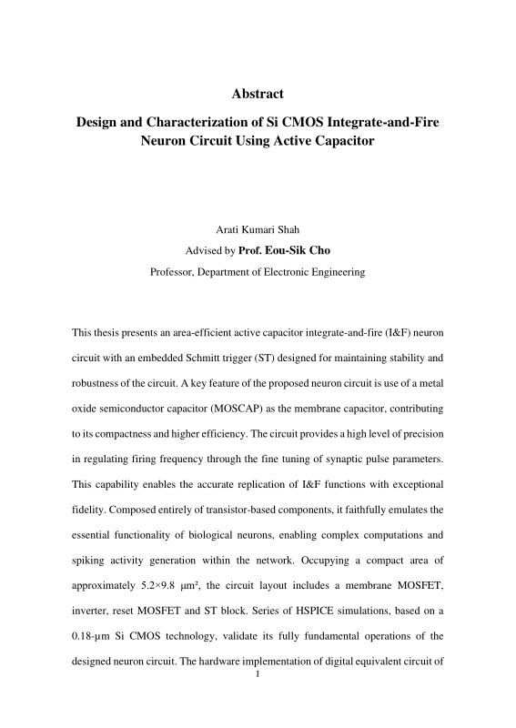
This thesis presents an area-efficient active capacitor integrate-and-fire (I&F) neuron circuit with an embedded Schmitt trigger (ST) designed for maintaining stability and robustness of the circuit. A key feature of the proposed neuron circuit is use of a metal oxide semiconductor capacitor (MOSCAP) as the membrane capacitor, contributing to its compactness and higher efficiency. The circuit provides a high level of precision in regulating firing frequency through the fine tuning of synaptic pulse parameters. This capability enables the accurate replication of I&F functions with exceptional fidelity. Composed entirely of transistor-based components, it faithfully emulates the essential functionality of biological neurons, enabling complex computations and spiking activity generation within the network. Occupying a compact area of approximately 5.2x9.8 μm², the circuit layout includes a membrane MOSFET, inverter, reset MOSFET and ST block. Series of HSPICE simulations, based on a 0.18-μm Si CMOS technology, validate its fully fundamental operations of the designed neuron circuit. The hardware implementation of digital equivalent circuit of the I&F neuron circuit has been realized using Field Programmable Gate Array (FPGA). The overall FPGA implementation allows the efficient simulation of I&F neuron behavior with digital integrated circuits, providing a platform for incorporating the schemed functions into complex computational neuroscience applications. A Zynq-Ultrascale MPSOC FPGA kit has been utilized for the implementation of hardware with a Verilog coding by VIVADO design suite.
This research provides a practical and innovative approach to designing compact and dependable neuron circuits suitable for seamless integration with synaptic devices, promising advancements in neural network simulations and neuromorphic engineering. Furthermore, the study addresses the imperative challenge of improving area efficiency of I&F neuron circuit, specifically focusing on controlling the size of shunt capacitor. Circuit simulations with 0.35-μm technology reveal efforts to optimize the neuron circuit area efficiency. The impact of area control over capacitors on spiking behaviors is meticulously examined, offering insights into the nuanced relationship between membrane capacitance and spiking frequency. This research contributes significantly to the field of spiking neural networks, offering not only a compact and efficient I&F neuron circuit but also insights into the broader landscape of hardware-based SNNs.
The findings underscore the potential application of the proposed circuit in data-intensive decision-making processes, emphasizing the importance of its high area efficiency. The integration of an Operational Transconductance Amplifier (OTA) subcircuit, validated through simulations, enhances output fidelity, demonstrating the circuit robust performance under varying conditions and offering valuable insights for hardware-centric SNN architectures. The research culminates in the hardware implementation of the equivalent digital I&F design module on FPGA platforms, further substantiating the practicality and applicability of the proposed circuit in real-world scenarios.*표시는 필수 입력사항입니다.
| *전화번호 | ※ '-' 없이 휴대폰번호를 입력하세요 |
|---|
| 기사명 | 저자명 | 페이지 | 원문 | 기사목차 |
|---|
| 번호 | 발행일자 | 권호명 | 제본정보 | 자료실 | 원문 | 신청 페이지 |
|---|
도서위치안내: / 서가번호:

우편복사 목록담기를 완료하였습니다.
*표시는 필수 입력사항입니다.
저장 되었습니다.
