 https://www.energy.gov/sites/prod/files/2020/06/f76/VTO_2019_APR_ELECTRIFICATION_FINAL_compliant_.pdf


권호기사보기
| 기사명 | 저자명 | 페이지 | 원문 | 기사목차 |
|---|
| 대표형(전거형, Authority) | 생물정보 | 이형(異形, Variant) | 소속 | 직위 | 직업 | 활동분야 | 주기 | 서지 | |
|---|---|---|---|---|---|---|---|---|---|
| 연구/단체명을 입력해주세요. | |||||||||
|
|
|
|
|
|
* 주제를 선택하시면 검색 상세로 이동합니다.
Title page
Contents
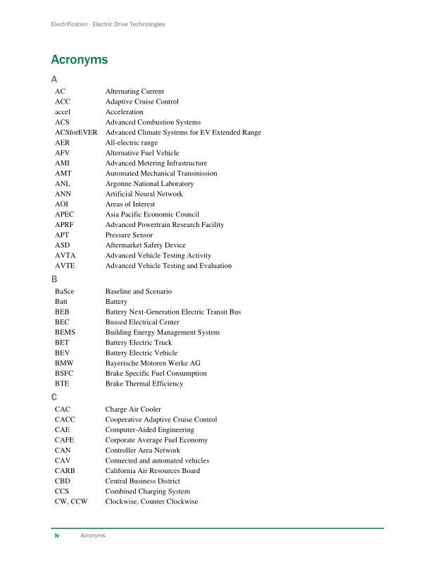
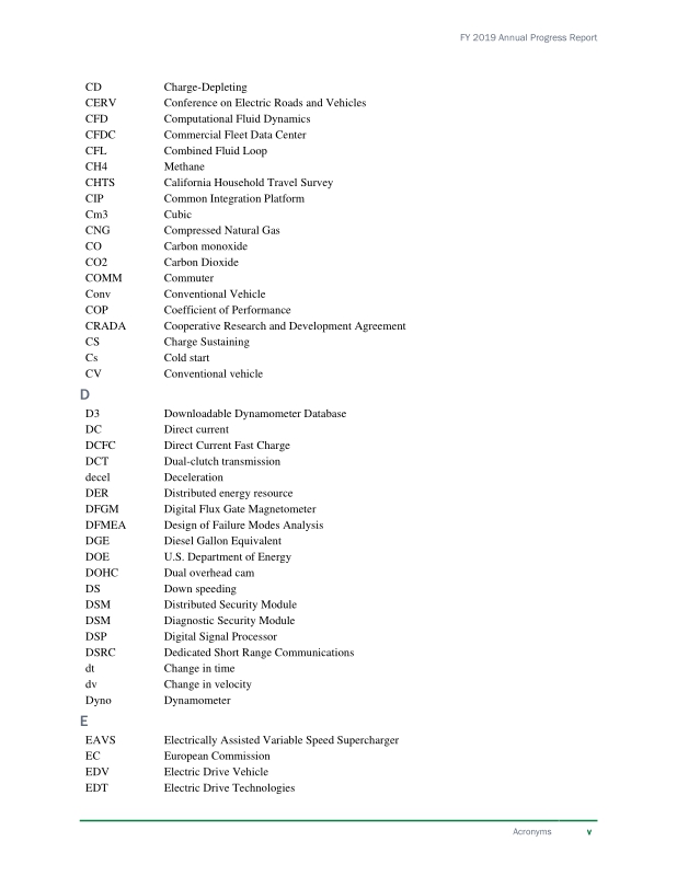
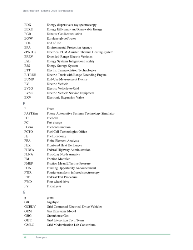
Acronyms 3
Executive Summary 12
Vehicle Technologies Office Overview 35
Electric Drive Technologies Program Overview 37
Grid and Infrastructure Program Overview 39
I. Electric Drive Technologies Research 49
I.1. Highly Integrated Power Module (ORNL) 49
I.2. High-Voltage, High-Power Density Traction Drive Inverter (ORNL) 56
I.3. High-Fidelity Multiphysics Material Models for Electric Motors (ORNL) 64
I.4. Non-Heavy Rare Earth High-Speed Motors (ORNL) 72
I.5. Integrated Electric Drive (ORNL) 82
I.6. Ultra-Conducting Copper (ORNL) 93
I.7. Power Electronics: Active Device and Passive Component Evaluation (SNL) 102
I.8. Bottom-Up Soft Magnetic Composites (SNL) 108
I.9. Component Modeling, Co-Optimization, and Trade-Space Evaluation (SNL) 114
I.10. Power Electronics: Vertical GaN Device Development (SNL) 121
I.11. Advanced Packaging Designs - Reliability and Prognostics (NREL) 129
I.12. Electric Motor Thermal Management (NREL) 136
I.13. Integrated Traction Drive Thermal Management (NREL) 143
I.14. Power Electronics Materials and Bonded Interfaces - Reliability and Lifetime (NREL) 150
I.15. Power Electronics Thermal Management (NREL) 158
I.16. Magnetics for Ultra-High Speed Transformative Electric Motor (Ames Lab) 167
I.17. Integration Methods for High-Density Integrated Electric Drives (University of Arkansas) 173
I.18. Design, Optimization, and Control of a 100kW Electric Traction Motor Meeting or Exceeding DOE 2025 Targets (Illinois Institute of Technology) 182
I.19. Cost Competitive, High-Performance, Highly Reliable (CPR) Power Devices on SiC (SUNY Polytechnic Institute) 190
I.20. Cost Competitive, High-Performance, Highly Reliable (CPR) Power Devices on GaN (SUNY Polytechnic Institute) 196
I.21. Device- and System-Level Thermal Packaging for Electric-Drive Technologies (Georgia Institute of Technology) 204
I.22. Next-Generation, High-temperature, High-frequency, High-efficiency, High-power-density Traction System (University of California, Berkeley) 213
I.23. Heterogeneous Integration Technologies for High-temperature, High-density, Low-profile Power Modules of Wide Bandgap Devices in Electric Drive Applications (Virginia Tech) 221
I.24. Integrated Motor and Drive for Traction Application (University of Wisconsin - Madison) 230
I.25. Multi-Objective Design Optimization of 100kW Non-Rare-Earth or Reduced-Rare Earth Machines (Purdue University) 239
I.26. Implementation of WBG devices in circuits, circuit topology, system integration as well as SiC devices (The Ohio State University) 247
I.27. Rugged WBG Devices and Advanced Electric Machines for High Power Density Automotive Electric Drives (North Carolina State University) 256
II. Electric Drive Technologies Development 260
II.1. High Speed Hybrid Reluctance Motor Utilizing Anisotropic Materials (General Motors LLC) 260
II.2. Dual Phase Soft Magnetic Laminates for Low-cost, Non/Reduced-Rare-Earth Containing Electrical Machines (GE Global Research) 268
II.3. Cost Effective 6.5% Silicon Steel Laminate for Electric Machines (Iowa State University) 275
II.4. Mapping the North American Light Duty Electric Vehicle (LDEV) Charging Market and Supply Chain: Assessment of Suppliers, Technology Developments and Gaps... 285
II.5. Highly Integrated Wide Bandgap Power Module for Next Generation Plug-In Vehicles (General Motors LLC) 293
II.6. V2G Electric School Bus Commercialization Project (Blue Bird Corporation) 299
III. Grid and Infrastructure Industry Awards 304
III.1. Emission Drayage Trucks Demonstration (ZECT I) 304
III.2. Zero Emission Cargo Transport II San Pedro Bay Ports Hybrid & Fuel Cell Electric Vehicle Project (South Coast Air Quality Management District) 312
III.3. Medium-Duty Urban Range Extended Connected Powertrain (MURECP), (Robert Bosch LLC) 321
III.4. Medium Duty Vehicle Powertrain Electrification and Demonstration (McLaren Engineering) 327
III.5. Wireless Extreme Fast Charging for Electric Trucks 332
III.6. Bidirectional Wireless Power Flow for Medium-Duty Vehicle-to-Grid Connectivity 336
III.7. Development and Demonstration of Medium-Heavy Duty PHEV Work Trucks (Odyne Systems) 343
III.8. Cummins Electric Truck with Range-Extending Engine (ETREE) (Cummins, Inc.) 349
III.9. Comprehensive Assessment of On-and Off-Board Vehicle-to-Grid Technology Performance and Impacts on Battery and the Grid (EPRI) 353
III.10. Enabling Extreme Fast Charging with Energy Storage (Missouri University of Science and Technology) 366
III.11. Intelligent, Grid-Friendly, Modular Extreme Fast Charging System with Solid-State DC Protection (NCSU) 372
III.12. Direct Current Conversion Equipment Connected to the Medium-Voltage Grid for XFC Utilizing a Modular and Interoperable Architecture (EPRI) 381
III.13. High-Efficiency, Medium-Voltage-Input, Solid-State-Transformer-Based 400-kW/1000-V/400-A Extreme Fast Charger for Electric Vehicles (Delta Electronics (Americas) Ltd) 384
IV. Grid and Infrastructure Grid Interoperability and Control 390
IV.1. Smart Vehicle-Grid Integration (ANL) 390
IV.2. Scalable Electric Vehicle Smart Charging Using Collaborative Autonomy (LLNL) 396
V. Grid and Infrastructure Fast Charging Enabling Technologies 402
V.1. Fast Charging: Interoperability and Integration Technologies (ANL) 402
V.2. Fast Charging: Grid Impacts and Cyber Security (INL) 407
V.3. Demand Charge Mitigation Technologies (NREL) 413
V.4. Smart Electric Vehicle Charging for a Reliable and Resilient Grid (NREL) 420
V.5. Smart Electric Vehicle Charging for a Reliable and Resilient Grid (Idaho National Laboratory) 426
V.6. Smart Electric Vehicle Charging for a Reliable and Resilient Grid (Recharge) (SNL) 432
V.7. Development of a Multi-port 1+ Megawatt Charging System for Medium-and Heavy-Duty Electric Vehicles (ORNL) 437
V.8. Development of a Multiport 1+Megawatt Charging System for Medium- and Heavy-Duty Electric Vehicles (NREL) 444
V.9. Development of a Multiport 1+ Megawatt Charging System for Medium and Heavy-Duty Electric Vehicles (ANL) 453
V.10. High-Power Inductive Charging System Development and Integration for Mobility (ORNL) 459
VI. Grid and Infrastructure High Power Wireless Charging 467
VI.1. High Power and Dynamic Wireless Charging of EVs (ORNL) 467
VI.2. High Power and Dynamic Wireless Charging for EVs (INL) 474
VII. Grid and Infrastructure Cyber Security 479
VII.1. Consequence-Driven Cybersecurity for High-Power Charging Infrastructure (INL) 479
VII.2. CyberX: Cybersecurity for Grid Connected eXtreme Fast Charging Station (Idaho National Laboratory) 486
VII.3. Threat Model of Vehicle Charging Infrastructure (ANL) 490
VII.4. Securing Vehicle Charging Infrastructure 492
Figure 1. Examples of EV Charging Stations 41
Figure I.1.1. Electrical layout of the half-bridge module 50
Figure I.1.2. Layer details and isometric view of IMS substrate 51
Figure I.1.3. Cross section of DBC (left), IMS (middle), and IMS with TPG (right) 51
Figure I.1.4. Steady-state thermal performance of DBC (left), IMS (middle), and IMSwTPG (right) 52
Figure I.1.5. Transient thermal impedance of SiC MOSFET dies placed on DBC (left), IMS (middle), and IMSwTPG (right) 53
Figure I.1.6. Thermal evaluation board (left); assembled substrate with cold plate, interconnects, and SiC MOSFETs (middle); setup for thermal characterization of DBC, IMS and... 53
Figure I.1.7. Thermal imaging results of IMS (left) and IMSwTPG (right) at 250W total power loss and 65℃ coolant temperature. 53
Figure I.1.8. IMS-based half-bridge power module 54
Figure I.1.9. Chip-to-chip and board-to-board interconnect examples with quilt packaging 54
Figure I.1.10. Test sample design for interconnect evaluation 54
Figure I.1.11. Fabricated silicon samples with quilt nodules 55
Figure I.2.1. A standard 3-phase inverter-based drive 57
Figure I.2.2. Segmented inverter-based drive 57
Figure I.2.3. Rearrangement of the segmented inverter-based drive 58
Figure I.2.4. PWM schemes for the segmented inverter-based drive to reduce the DC bus ripple current: (a) phase-shifted carrier-based schemes, (b) space vector modulation with... 58
Figure I.2.5. Simulated operating waveforms for the segmented inverter with a capacitor ripple current of 17.5Arms (a) and standard inverter with a capacitor ripple current of 62.1Arms... 59
Figure I.2.6. Comparison of normalized capacitor ripple current (a) and busbar current (b) vs. modulation index for 3-phase and segmented inverters at various power factors 60
Figure I.2.7. Block diagram for a 5-phase inverter (a) and simulation waveforms for switching at m=0.65 and pf=0.9 (b) 60
Figure I.2.8. Block diagram (a) and simulation waveforms for a symmetrical 6-phase inverter at m=0.65 and pf=0.9 (b) 61
Figure I.2.9. Block diagram (a) and simulation results for an asymmetrical 6-phase inverter at m=0.65 and pf=0.9 (b) 61
Figure I.2.10. Block diagram for driving cycle-based DC bus capacitor life-expectancy prediction and sizing tools 62
Figure I.2.11. Modeling results for a film capacitor under US06 driving cycle (left) and FUDDS (right) 62
Figure I.2.12. Inverter power stage design (left) and power module baseplate temperature profile (right) 63
Figure I.3.1. Nine-magnet permanent magnet array for accurate 3-axis demagnetization testing of low-energy- product and HRE-free permanent magnets. Two 3-axis magnetic field... 66
Figure I.3.2. Simulation comparison of single cubic magnet measurement versus nine-magnet array measurement. The intrinsic curve is the permanent magnet data input into the... 66
Figure I.3.3. One-eight section cutaway simulation of the optimized permanent magnet testing fixture. The peak aperture airgap flux density is 1.8T with uniformity of better than 1%... 68
Figure I.3.4. Disassembled permanent magnet array assembly 68
Figure I.3.5. Permanent magnet test fixture subassemblies and components; (Left) One of the two excitation coils after removal from bobbin. (Center) ferromagnetic yoke with excitation... 69
Figure I.3.6. Complete permanent magnet testing system including power supply, inverter, magnetic field sensors, current sensors, and oscilloscope 69
Figure I.3.7. Comparison of measured AlNiCo 8HC hard and easy axis magnetization characteristics; (Right) normal curves, (left) intrinsic curves. A computed estimate of the expected... 70
Figure I.4.1. Proposed rotary transformer-based excitation system with resonant compensation only on the primary side 73
Figure I.4.2. Robustness of the field current against the variation of field winding resistance due to temperature (for a temperature swing from −50 to 150℃) 73
Figure I.4.3. Resistance of the HRE-free outer rotor SPM to demagnetization under 3-phase short circuit at 20,000rpm 74
Figure I.4.4. Mechanical assembly and stress analysis at 20,000rpm 75
Figure I.4.5. AC loss in winding and eddy current loss in permanent magnets at 100kW and 20,000rpm operation 78
Figure I.4.6. Thermal simulation results at 20krpm with high thermal conductivity winding potting, winding spray cooling, slot wedge liquid cooling, and rotor liquid cooling (Refer to... 79
Figure I.4.7. Analyzed motor topologies 79
Figure I.4.8. Impact of winding conductivity on the motor active volume 80
Figure I.4.9. Impact of winding conductivity on the speed range and efficiency 80
Figure I.5.1. Motor and inverter integration techniques: (a) radial housing mount, (b) radial stator mount, (c) axial endplate mount, (d) axial stator mount 83
Figure I.5.2. One-sixth of 2016 BMW-i3 stator 84
Figure I.5.3. DBC structure for thermal simulation 84
Figure I.5.4. Power loss data: (a) experimental motor power loss; (b) inverter power loss (simulation-based) 85
Figure I.5.5. Identification of required thermal performance of radial stator mount IMD system. htc = heat transfer coefficient 85
Figure I.5.6. Capacitance density of the selected capacitor 86
Figure I.5.7. Experimental setup 87
Figure I.5.8. Change in ESR and capacitance with DC bias voltage (f = 1kHz, T = 23℃) 88
Figure I.5.9. Change in ESR and capacitance of different capacitor technology in terms of frequency, bias voltage, and temperature 89
Figure I.5.10. The volume of the selected capacitor technologies compared with that of a 2016 BMW-i3 450V 475uF film capacitor 91
Figure I.6.1. Schematic illustration of the process flow for producing Cu-CNT-Cu multilayer composite tapes 95
Figure I.6.2. Scanning electron microscopy images and G-band intensity variations on single-walled CNT-coated copper tapes at various inclination angles during ultrasonic spray... 96
Figure I.6.3. Scanning electron microscopy images displaying the shear-induced alignment of CNTs with increased CNT loading on copper tapes 96
Figure I.6.4. (Left) Electrical properties of single-layer and three-layer Cu-CNT-Cu composite architectures as a function of temperature ranging from 0 to 120℃, displaying reduced... 97
Figure I.6.5. Energy diagram showing the density of states for metallic, semiconducting, and Cu-doped semiconducting CNTs (left panel). Z-contrast STEM image of a Cu-CNT-Cu... 98
Figure I.6.6. Cross-sectional schematic illustration of the three topologies of heavy rare-earth-free permanent magnet traction motors 99
Figure I.6.7. Reduction in active volume as a function of winding conductivity for different motor topologies 99
Figure I.6.8. Photograph of the newly designed roll-to-roll CNT deposition system 100
Figure I.7.1. Oxygen vacancy migration under applied bias can lead to degradation of ceramic capacitors 103
Figure I.7.2. The evaluation of prototype devices in a custom testbed can inform both device designers on the strengths/weaknesses of their prototypes, as well as validate device... 104
Figure I.7.3. Schematic for WBG device testbed with embedded motor control 104
Figure I.7.4. The lifetime of DC capacitors can be increased through the implementation of a bipolar switching scheme 105
Figure I.7.5. Design layout for capacitor test setup which allows for stress and evaluation of a population of 40 capacitors under bipolar switching 105
Figure I.7.6. Breadboard of 3-phase DC motor drive power stage (left) and embedded controller (right) 106
Figure I.7.7. (left) Thermal image of one leg of the power stage showing the temperature of power switches (centered at the crosshairs) and gate driver (just below the crosshairs)... 107
Figure I.8.1. Temperature-dependent XRD data of commercially available mixed phase iron nitride powder and its conversion to nearly phase pure Fe₄N 109
Figure I.8.2. 1,6-hexanediamine 110
Figure I.8.3. N,N-diglycidyl-4-glycidyloxyaniline 110
Figure I.8.4. Magnetic composite toroidal cores wound for B-H analysis 110
Figure I.8.5. B-H hysteresis loop for a magnetic composite toroid. This hysteresis loop was collected at a frequency of 10kHz 111
Figure I.8.6. 3D printed magnetic composite rotor (1/6 of total rotor design) 111
Figure I.8.7. 4-aminophenyl sulfone 112
Figure I.8.8. Three differently-sized magnetic composite rotor teeth and a magnetic composite toroid 112
Figure I.9.1. Comparison of power loss in SiC MPS, GaN PiN, and GaN JBS diodes showing (left) preferred device as a function of voltage and frequency at 50% duty cycle, and (right)... 116
Figure I.9.2. Comparison of Ron in MOSFETs made in Silicon, SiC, and GaN showing (left) the device structure and (right) the predicted results 117
Figure I.9.3. Circuit topology for co-optimization 117
Figure I.9.4. Candidate design considers a flat integrated form factor that includes module and DC link capacitor 118
Figure I.9.5. Module volume estimate as a function of voltage and frequency for Ceramic X7R and Ceralink Capacitors 118
Figure I.9.6. Co-optimization results for (left) 10kW boost converter and (right) 100kW inverter module + capacitor 119
Figure I.10.1. (top) Schematic drawing of JBS diode. (bottom) Schematic drawing of Trench MOSFET 121
Figure I.10.2. Simulated reverse-bias curves of GaN Schottky diodes using various transport models (courtesy of Lehigh University) 122
Figure I.10.3. Schematic drawings of (top) trench MOSFET and (bottom) double-well MOSFET 123
Figure I.10.4. (top) IV curves of GaN Schottby Barrier Diodes, and (bottom) extracted ideality factors of the same diodes 124
Figure I.10.5. (top row) Simlulated breakdown voltage and (bottom row) on-resistance of GaN JBS diodes. Left column is a design with a narrow current-carrying channel, while right... 125
Figure I.10.6. Simulated Baliga Figure of Merit for JBS diodes with three different p-layer widths 125
Figure I.10.7. TCAD simulations of D-MOSFETS, examine four design parameters: (top left) JFET region width, epilayer (drift layer) doping (top right), current spreading layer doping... 126
Figure I.10.8. (left) Schematic drawing of T-MOSFET. (middle) Simulated internal electric field of the same device. (right) simulated breakdown characteristic of the same device 126
Figure I.11.1. A traditional power electronics package (left), and double-sided-cooled power electronics packages from Toyota and General Motors (right) 130
Figure I.11.2. Power device within a second-generation Chevy Volt (left), and example double-sided cooling structure (right) 131
Figure I.11.3. Traditional package with metalized polyimide substrate (left), and with polyimide substrate bonded directly to baseplate/heat exchanger with no bottom metallization... 132
Figure I.11.4. Double-sided cooled package with polyimide substrate (left), and with stacked devices in a 3D package design (right) 132
Figure I.11.5. Manufacturing process for a traditional power electronics module (top), and a simplified process for the novel power electronics package (bottom) 133
Figure I.11.6. Sample design with QP 134
Figure I.12.1. Overview of ASTM D5470 method for measuring the thermal resistance of a sample placed between two metering blocks 138
Figure I.12.2. Example analysis for locating temperature measurement locations within bottom metering block. Example temperature profile through metering block showing uniform... 139
Figure I.12.3. Example analysis for including a copper spreader to the metering block with different metering block materials. Drawing of metering block with copper spreader (left)... 140
Figure I.12.4. Constructed experimental hardware inside environmental chamber 141
Figure I.13.1. Electric motor and power electronics integration concepts: (a) Separate enclosures for motor and power electronics, (b) Power electronics mounted or distributed... 144
Figure I.13.2. Experimental setup for jet impingement heat transfer characterization: (a) General view of large fluid test loop, (b) Large fluid test loop schematic 144
Figure I.13.3. Electric machine with mounted heat target assembly within the end-windings (Computer-aided design (CAD) model by Emily Cousineau, NREL) 145
Figure I.13.4. FEA thermal simulations of a single slot of stator windings in ANSYS: (a) Heat flux distribution, (b) Temperature distribution 145
Figure I.13.5. ATF jet impingement on heated target 146
Figure I.13.6. Experimentally measured convective heat transfer coefficients for 50℃ ATF at various jet impingement velocities and cooled-surface temperatures 147
Figure I.13.7. CFD modeling of orifice and fan-shaped jet impingement on heated copper target 147
Figure I.14.1. Pressureless sintering profile at VT (left) and NREL (right) 151
Figure I.14.2. Circular coupons (Φ25.4mm) for reliability evaluation - Cu (bottom) bonded to Invar (top) using sintered silver 152
Figure I.14.3. C-SAM images of pressureless sintered silver samples fabricated at VT (left and center) and NREL (right) 152
Figure I.14.4. Pressure-assisted sintering profile 152
Figure I.14.5. C-SAM images of pressure-assisted sintered silver samples fabricated at VT. Bond diameter of 22mm (left), 16mm (center), and 10mm (right) 153
Figure I.14.6. Round sintered silver samples arranged on a thermal platform for thermal cycling 153
Figure I.14.7. C-SAM images of pressureless sintered silver before (left) and after 10 thermal cycles (right) - Cu-side images (top) and Invar-side images (bottom) 154
Figure I.14.8. C-SAM images of pressure-assisted sintered silver before (left) and after 100 thermal cycles (right), Cu-side images (top) and Invar-side images (bottom) 155
Figure I.14.9. Crack growth in pressure-assisted samples (3MPa) 155
Figure I.14.10. Cross-sectional image of a pressure-assisted sintered silver sample 156
Figure I.14.11. Strain energy density results of sintered silver samples 156
Figure I.15.1. Schematic showing the dielectric fluid cooling strategy for a planar-style module 159
Figure I.15.2. CFD results showing the effects of varying the fin thickness (left), fin height (middle), and the slot jet width (right) 160
Figure I.15.3. CFD temperature contours for the optimal fin and slot jet design using the device scale model. Model predicts 220℃ maximum junction temperature at 716 W/cm²... 160
Figure I.15.4. CFD-predicted flow distribution for the 12 slot jets. A ±5% flow variation is predicted 161
Figure I.15.5. CAD drawing of the heat exchanger designed to cool 12 (25mm²) devices (left). 3D printed heat exchanger fabricated for experimental validation (right). Total volume... 161
Figure I.15.6. Temperature contours for inverter-scale (12 devices) CFD simulations for 2.2kW of heat dissipation (716W/cm² per device) and total flow rate (Alpha 6 fluid) of 4.1lpm... 162
Figure I.15.7. Image of the finned (wf = 0.2mm, wc = 0.43mm, and hf = 4mm) heat spreader (left) and cartridge heater block (middle). FE-analysis-predicted temperatures for the... 162
Figure I.15.8. Picture of the dielectric fluid flow loop fabricated and used to measure the thermal performance of the dielectric fluid heat exchanger. The flow loop can accommodate... 163
Figure I.15.9. Schematic of the 1D transient thermal FEA model (left). FEA temperature versus time results for a simulated short-circuit fault condition (right) 164
Figure I.15.10. Predicted thermal resistance for the double-side-cooled module design indicating substantial thermal performance enhancements compared to the single-side-cooled design 164
Figure I.16.1. Dependence of coercivity on grain size 168
Figure I.16.2. Micromagnetic simulation of the demagnetization field near the permanent magnets in motor 169
Figure I.16.3. MH curves of the bulk magnet prepared using feedstock powders that were ball-milled for different time. The longer the ball milling hours, the finer the particle size 169
Figure I.16.4. MH curves of the assemblies listed in Table I.1.16.1 170
Figure I.16.5. a) the large melt-spinner capable of producing 500 gram thin sheet steel; b) the 10 mm ribbon of 6.5% Si steel prepared using only 10 gram of ingot; c) The new... 171
Figure I.17.1. Simplified SiC CMOS gate driver schematic and layout with programmable drive strength 176
Figure I.17.2. Simplified SiC NMOS gate driver schematic and layout with programmable drive strength 177
Figure I.18.1. Representative interior permanent magnet synchronous machines from optimization Pareto front 184
Figure I.18.2. Pareto fronts to identify target performance gaps using state of the art motor topologies and materials 185
Figure I.18.3. Magnetic only topology optimization, (a) design domain, (b) synchronous reluctance rotor, (c) interior permanent magnet rotor with fixed permanent magnet 186
Figure I.18.4. Synchronous reluctance rotor magneto-structural topology optimization results for (a) formulation I 4,000RPM, (b) formulation II 4,000RPM, (c) formulation I 12,000RPM,... 188
Figure I.18.5. Interior permanent magnet synchronous machine rotor magneto-structural topology optimization with fixed position and size permanent magnet, (a) normalized electrical... 189
Figure I.18.6. Multi-layer IPM rotor verification of the proposed design approach, (a) cross-section of barriers and magnets, (b) flux density distribution at no-load 189
Figure I.19.1. Cross-sectional view of proposed 1.2kV 4H-SiC MOSFETs 191
Figure I.19.2. Optimization of the JFET doping concentration to minimize the on-resistance and electric field in gate oxide and PN junction 191
Figure I.19.3. Optimization of the JFET width to minimize the on-resistance and electric field in gate oxide and PN junction 192
Figure I.19.4. Top view for Mask 192
Figure I.19.5. 1st lot fabrication status 193
Figure I.20.1. AFM scans of (a) AlGaN/GaN on sapphire and (b) AlGaN/GaN on Si 198
Figure I.20.2. in situ curvature measurement during growth 198
Figure I.20.3. Output and gate leakage characteristics for HEMT on sapphire. Device Dimensions: Wg=150μm; Lg=7μm; Lgs=4μm; Ldg=10μm; Lds=21μm 199
Figure I.20.4. Output and gate leakage characteristics for HEMT on sapphire. Device Dimensions: Wg=150μm; Lg=7μm; Lgs=4μm; Ldg=10μm; Lds=21μm 199
Figure I.20.5. Frequency-dependent C-V measurements for samples annealed at (a) 350℃ for 1 min, (b) 350℃ for 10 min, (c) 350℃ for 20 min, (d) 600℃ for 1 min, (e) 475℃ for 10 min,... 200
Figure I.20.6. C-V measurement data collected at 100kHz AC signal. The arrows indicate the direction of the DC bias sweep. Insets show zoomed in area of hysteresis to show changes in... 201
Figure I.20.7. EDS elemental maps showing the spatial distribution of (a) O in the as-deposited sample, (b) Al in the as-deposited sample, (c) O in the sample annealed at 350℃ for... 202
Figure I.21.1. Illustration of steps for commercial stochastic foam characterization 206
Figure I.21.2. Comparison of ERG foam versus AM foam (left) and reduced computational domains (right) 206
Figure I.21.3. Pressure drop per unit length (left) and Nusselt number (right) for the ERG and AM samples 207
Figure I.21.4. Nusselt numbers recalculated with varying TIM thermal conductivities 208
Figure I.21.5. 50mm × 50mm prototype of AlSiC heat sink bonded to AlN and Al foam with liquid header 208
Figure I.21.6. (a) Assemble packaged prototype (b) Liquid coolant loop setup showing essential sensors and DAQ 209
Figure I.21.7. Failed Cu-invar bond 209
Figure I.21.8. SEM and EDS results of Cu-Al bond between a) Cu-Invar coupons b) Invar-Invar coupons c) Cu-Cu coupons 210
Figure I.21.9. (a) Maximum Shaft Torque, (b) Maximum Shaft Power, (c) Maximum Stator Winding Current and (d) Maximum Efficiency, with a temperature threshold of 200℃ and for... 211
Figure I.21.10. (a) Maximum Shaft Torque, (b) Maximum Shaft Power, (c) Maximum Stator Winding Current and (d) Maximum Efficiency, with a temperature threshold of 200℃, a fixed... 211
Figure I.22.1. Comparison in output waveforms of a conventional two-level design (left), and a 9-level, dual-interleaved FCML design (right). The latter are from results in, and illustrate... 214
Figure I.22.2. Top: schematic and current waveforms for a dual-interleaved, 10-level FCML inverter. Bottom: hierarchical control strategy and system diagram of paralleled converters of... 215
Figure I.22.3. Left: measured overshoot of the commutation loop in this design. Right: measured experimental performance of the prototype inverter module across various load... 216
Figure I.22.4. Left: an annotated hardware prototype of the 10-level, dual-interleaved inverter module for this project. Right: a 9-module, segmented inverter paralleled across three... 217
Figure I.22.5. Left: experimental setup showing the thermal test assembly for this air-cooled inverter iteration. Right: CFD results showing relatively a relatively uniform pressure front... 218
Figure I.22.6. Nonlinear simulation of the flying capacitor voltages during dc bus startup 219
Figure I.22.7. Calorimetric test setup used in evaluating large-signal loss characteristics for passive devices. The entire assembly is loaded into a temperature-controlled chamber during... 219
Figure I.23.1. A schematic of the hardware to be developed in this project 222
Figure I.23.2. Summary of recommended high temperature packaging materials for power modules 223
Figure I.23.3. High temperature gate driver IC from Cissoid 223
Figure I.23.4. Air-core inductors 224
Figure I.23.5. The layout design of a 1.2kV, 149 A SiC MOSFET planar module with double-side cooling 226
Figure I.23.6. Terminals of the power module for gate driver and current sensor 226
Figure I.23.7. (a) Equivalent circuit of power MOSFET model, and (b) Current sensing with short-circuit protection and current reconstruction 227
Figure I.23.8. Sensor waveforms (scaled) in comparison to the actual current waveforms 227
Figure I.23.9. Reconstructed current waveform 227
Figure I.23.10. Short-circuit protection 227
Figure I.24.1. Integrated Modular Motor Drive (IMMD) concept 232
Figure I.24.2. IMD Topologies 233
Figure I.24.3. Alternative traction inverter drive configurations: a) VSI excitation; and b) CSI excitation 234
Figure I.24.4. Typical line-to-neutral voltage waveforms for (a) VSI and (b) CSI 234
Figure I.24.5. Typical switch voltage and current waveforms for (a) VSI and (b) CSI 236
Figure I.24.6. Electric machine categorization segregating machine types with and without permanent magnets 236
Figure I.24.7. Flux-weakening performance comparison of the CSI-excited and VSI-excited SPM machines for CPSR=6.25 237
Figure I.25.1. Homopolar AC Machine 241
Figure I.25.2. HAM magnetic equivalent circuit 241
Figure I.25.3. HAM phase MMF waveforms 242
Figure I.25.4. Preliminary HAM Pareto-optimal front 243
Figure I.25.5. Preliminary HAM design 243
Figure I.25.6. (a) Surface meshed linear materials and (b) volume-meshed nonlinear materials for a PMSM model 244
Figure I.25.7. Pareto-optimal front from an MoM-based optimization 245
Figure I.26.1. SiC MOSFET Reliability Issues 247
Figure I.26.2. Key Partnerships 248
Figure I.26.3. Gate leakage current-voltage characteristics at three different temperatures 250
Figure I.26.4. Weibull distribution of vendor E' for four different gate voltages at 28℃ and 175℃ 251
Figure I.26.5. Degradation of the 3rd quadrant ID-VD characteristics for built-in body diode of one selected 1.7kV SiC DMOSFET from each vendor 252
Figure I.26.6. Reverse bias characteristics at gate voltage of VGS = 0V of one selected 1.7kV SiC DMOSFET from each vendor at room temperature before and after stress of the... 252
Figure I.26.7. Time-dependent threshold voltage shifts for (a) positive bias-stress of +20V, (b) +30V, and (c) negative bias-stress of -10V for 50 hours 253
Figure I.26.8. Temperature-dependent (a) threshold voltage values and (b) ID-VG transfer characteristics of device E' and C 253
Figure I.26.9. Block diagram of gate drive circuit 254
Figure I.26.10. Load transient response, Propagation delay waveform, Relationship between the output voltage levels of outputs and switching frequency 254
Figure I.27.1. Design-I 258
Figure I.27.2. Design-II 258
Figure I.27.3. Design-III 258
Figure I.27.4. Short circuit at 18,000rpm 258
Figure I.27.5. Short circuit at 18,000rpm 258
Figure I.27.6. Short circuit at 18,000rpm 258
Figure I.27.7. Slotless motor using thermal plastic 259
Figure I.27.8. Slotless motor using Alumina 259
Figure II.1.1. Variant 1, 2, and 3 rotors shown from left to right 262
Figure II.1.2. Variant 1, 2, and 3 stators shown from left to right 263
Figure II.1.3. Rotor casting simulations for improved Al-Cu interface strength 263
Figure II.1.4. Average rotor bar improvement from baseline (Casting #15) based on pull force. Casting numbers represent different parameters in the design of experiment 263
Figure II.1.5. Cost analysis of Variants 1, 2, and 3. Variant 1 only was estimated to be below the DoE cost target of $4.7/kW 264
Figure II.1.6. Stress life curves for materials "A", "B", and "C" 265
Figure II.1.7. Example of fracture analysis with SEM for material A, sample #2 265
Figure II.1.8. Rotor bar casting sample 266
Figure II.1.9. X-ray CT scanning results from rotor bar sample 266
Figure II.2.1. Illustration of the dual phase structure in a laminate used to manufacture a SynRel machine. The left image shows where the non-magnetic (orange) regions are... 269
Figure II.2.2. Manufacturing sequence for prototypes containing dual phase magnetic laminates 270
Figure II.2.3. a) Fully assembled full-scale prototype motor. b) exterior dimensions of the prototype motor 271
Figure II.2.4. Full-scale prototype motor on a dynameter test stand 272
Figure II.2.5. Measured continuous shaft torque and power output of the full-scale dual phase synchronous reluctance prototype made from the dual phase laminate rotor 273
Figure II.2.6. Measured efficiency of the full-scale dual phase synchronous reluctance prototype made from the dual phase laminate rotor 273
Figure II.3.1. Magnetization vs. applied field at different temperature of the bulk magnet fabricated using the newly developed CIP process. Note that the coercivity increases with... 277
Figure II.3.2. Photo of 5wt% epoxy bonded core after curing. The surface epoxy coat has not been applied 279
Figure II.3.3. Iron loss of epoxy bonded, flake core ring samples as a function of flux density for a number for frequencies (a) 5wt% epoxy, flux area by dimension; (b) 3wt% epoxy,... 280
Figure II.3.4. (a) MgO laminated ring, the bright features are MgO agglomerations. (b) Cross-section optical image of the MgO laminated ring sample, the dark strips are MgO layers,... 280
Figure II.3.5. Magnetic properties of MgO laminated rings. (a) Flux density as a function of magnetic field for both the DC and AC400Hz condition using dimension method; (b) flux... 281
Figure II.3.6. Picture of the prototype rotor (left) and stator (middle), and fully assembled motor 281
Figure II.3.7. Motor test setup at UTRC 282
Figure II.3.8. Comparison between the predicted back EMF results and the actual measurements 283
Figure II.4.1. Organizations That Are Publicly Held and Actively Engaged in the NA EVSE Supply Chain, Ranked by Annual Revenues (Calendar Year 2018) 288
Figure II.4.2. NA EVSE Supply Chain Organizations, By Product or Service Category (Represents 170 organizations, both public and private.) As of July 2019 289
Figure II.5.1. Automotive SiC power module with 900V SiC die 295
Figure II.5.2. Switch resistance: (left) measured through pcb flex circuit (right) measured through module terminals 295
Figure II.5.3. Hardware set-up for the thermal impedance measurements 296
Figure II.5.4. Thermal impedance curves for Vgs=-8V: (left) Zth for switch UHI, (middle) Zth for switch VHI, (right) Zth for switch WHI 296
Figure II.5.5. Equivalent 6th order Cauer impedance network to represent thermal impedances 297
Figure II.6.1. Dynamometer results for bus P1' vs. bus P1. Provided by NREL based on P1' dynamometer testing on May 29, 2019 302
Figure III.1.1. TransPower EDD Battery Electric Trucks 306
Figure III.1.2. US Hybrid Battery Electric Truck No. 1 307
Figure III.1.3. US Hybrid Battery Electric Truck No. 2 307
Figure III.1.4. TransPower CNGH-1 308
Figure III.1.5. Route containing hills during Q4 2018 tests 309
Figure III.1.6. TransPower - CNGH-2 (APU view) 309
Figure III.1.7. (Omit) 309
Figure III.1.8. TransPower - CNGH-2 with trailer 309
Figure III.1.9. US Hybrid LNGH 310
Figure III.1.10. US Hybrid LNGH pulling a container for TTSI 310
Figure III.2.1. CTE/Kenworth Fuel Cell Truck 313
Figure III.2.2. TransPower Fuel Cell Truck in Foreground & CNG Truck in Background 313
Figure III.2.3. U.S. Hybrid Truck: Design to Fabrication 313
Figure III.2.4. Kenworth/BAE - CNG Hybrid System Architecture 314
Figure III.3.1. Mutual verification of simulation and powertrain dyno measurements 322
Figure III.3.2. Fluids box redesign to improve space utilization, ease assembly on truck chassis 323
Figure III.3.3. Consolidation of separate 12V 24V and HVIL fuse relay boxes into one 323
Figure III.3.4. Performance vs. Speed simulation results in different modes including transmission spin losses 325
Figure III.3.5. 1MEV to Powersplit Transient including Hybrid Start 325
Figure III.3.6. 1MEV to Powersplit Transient including Hybrid Start 326
Figure III.4.1. Hybrid System vehicles in Build Shop 329
Figure III.4.2. Complete eAxle System on McLaren Test Rig 329
Figure III.4.3. 1st Design Demonstrator On Real World Commissioning Drive 330
Figure III.4.4. Vehicle, Being Returned to Shop for Adjustments/Updates 330
Figure III.5.1. WXFC project activities 333
Figure III.5.2. Project design and implementation approach 333
Figure III.5.3. System block diagram 334
Figure III.6.1. System level diagram of the proposed architecture for the bidirectional wireless charging system 338
Figure III.6.2. System level diagram of the proposed architecture for the bidirectional wireless charging system 338
Figure III.6.3. System level diagram of the proposed architecture for the bidirectional wireless charging system 338
Figure III.6.4. Primary and secondary coils with their resonant tuning components (a) and Bode 100 frequency response analyzer used for voltage gain characterization of the system 339
Figure III.6.5. Resonant voltage gain of the system using the analytical model (a) and the experimental validation (b) 339
Figure III.6.6. Resonant voltage gain of the system using the analytical model (a) and the experimental validation (b) 340
Figure III.6.7. Experimental test results for G2V mode with 20kW power transfer to the vehicles-side battery emulator: Operational waveforms (a) and power analyzer measurements (b) 340
Figure III.6.8. Experimental test results for V2G mode with 20kW power transfer to the primary-side DC link 341
Figure III.7.1. Odyne powertrain configuration 344
Figure III.7.2. Odyne hybrid architecture 345
Figure III.7.3. Odyne / Oak Ridge HIL powertrain test stand 346
Figure III.7.4. Torqeedo 11.6kWh battery pack 347
Figure III.7.5. Test chassis design layout 347
Figure III.7.6. Completed test chassis and hydraulic test stand 348
Figure III.8.1. ETREE powertrain test cell located at Cummins Technical Center, Columbus, Indiana 351
Figure III.8.2. ETREE alternate battery- drivers side enclosure (shown without cover) 351
Figure III.9.1. NRTC Lab Equipment Set Up with SPIN Rack System 357
Figure III.9.2. Power Analyzer Test Trace Showing Sequential Execution of All of the SPIN Operating Modes 357
Figure III.9.3. SPIN DC Communications Control Module (CCM) with J1772 Combo Coupler Assembly 358
Figure III.9.4. IoTecha EVCC and SECC Card Facilitates SPIN to PHEV DC Charging Communications 358
Figure III.9.5. SPIN Product Concept 3D-Layout including DC CCM and Charging Cable 359
Figure III.9.6. SPIN Application Scenarios being Designed for Verification 360
Figure III.9.7. SPIN Integrated Ecosystem Software Architecture: In-Cloud, On-Vehicle and On-SPIN 360
Figure III.9.8. Combined IEEE2030.5 and DIN 70121 Communications Sequence Diagram 362
Figure III.10.1. Block-diagram schematic of the XFC station 367
Figure III.10.2. Hierarchical control architecture 367
Figure III.10.3. Comparison between full model and estimator for two CCCV cycles at 1C with constant diffusivities 368
Figure III.10.4. Experimental results for open-circuit potential and solid-phase lithium diffusivity of half-cells 369
Figure III.10.5. Prototype module to construct cascaded H-bridge 369
Figure III.10.6. Virtual inertia control scheme 370
Figure III.10.7. Improved performance of the NN-MPC virtual inertia compared to PI controllers 370
Figure III.10.8. Bus voltage and current without (Case I) and with (Case II) reactive power injection 371
Figure III.11.1. System Layout showing the key components: MV SST, DC distribution network, and DC node that contains the DC/DC converter and vehicle interface 373
Figure III.11.2. MV SST Converter topology. The SST is made up of 6 Levels connected in input-series output-parallel configuration 375
Figure III.11.3. [Left] Small-scale prototype of the SST stage used for control validation [Right] Experimental results showing the behavior of the single module connected to an ac... 376
Figure III.11.4. Fault scenarios under investigation 377
Figure III.11.5. [Left] Advanced thermosyphon design and operating principle [Right] First batch of manufactured advanced thermosyphon for breaker B1 378
Figure III.11.6. [Left] IGCT stack for 500 A class breaker B2 with forced air cooling system [Right] Air flow analysis for design validation of cooling system for 500 A class breaker B2 378
Figure III.11.7. Example of high di/dt current transient during a short circuit event 379
Figure III.11.8. [Left] Mechanical design of SS DCCB B1; [Right ] Mechanical design of power stack for unidirectional SS DCCB B2 379
Figure III.13.1. XFC System Architecture 385
Figure III.13.2. Circuit Diagram of Power Module 385
Figure III.13.3. Picture of an SST Module at left, and Charging Controller (Buck) Module at right 386
Figure III.13.4. SST's AC/DC Stage Waveforms (CH1 brown: Vph, CH2 blue: VAC, CH3 purple: VL, CH4 green: IAC) 387
Figure III.13.5. SST's DC/DC Stage Waveforms (CH1 brown: VGS, CH2 blue: VDS, CH3 purple: ILr, CH4 green: VCr) 387
Figure III.13.6. 1-Phase Series SST and Buck Module Test Setup (up to 45-kW) 388
Figure III.13.7. 1-Phase Series SST and Buck Module Efficiency Test Result (up to 45-kW) 388
Figure IV.1.1. SAE J1772 charge connector w/DEVA 394
Figure IV.1.2. SpEC module 2.0 alpha board 394
Figure IV.1.3. Multi-unit sub-meter (w/o current sensors) 394
Figure IV.2.1. ADMM allows groups of distributed computers to jointly solve optimization problems 398
Figure IV.2.2. Charging station demand and net load for an 8,000 kVA distribution grid based on CAISO data 400
Figure IV.2.3. 100 CS show valley filling; net load from 6-10 pm cannot be flattened by reducing charging load 400
Figure V.1.1. 200kW DC EVSE Interoperability Testing 403
Figure V.1.2. BTC Power SLAC-based Communication 404
Figure V.1.3. BTCP DCFC Communication Log 404
Figure V.1.4. Comemso EV Charge Analyzer 405
Figure V.2.1. 350-kW XFC charging a 2014 BMW i3 in INL's Electric Vehicle Infrastructure Lab 408
Figure V.2.2. 350-kW XFC charging a New Flyer 60-foot electric transit bus in INL's Electric Vehicle Infrastructure Lab 408
Figure V.2.3. Efficiency of the 350-kW XFC 409
Figure V.2.4. Charge profile of the 2014 BMW i3 connected to the 350-kW XFC 410
Figure V.2.5. Charge initialization ramp-up characteristics when charging with a 350kW capable XFC 410
Figure V.2.6. Comparison of charge event initialization and power ramp-up: 50kW DCFC and 350kW XFC 411
Figure V.2.7. Power ramp-down at the end of a charge on the 350-kW XFC 411
Figure V.2.8. Schematic of vehicle emulator that uses the XFC's Combined Charging System (CCS) connector 412
Figure V.3.1. Energy envelop of each device and aggregated energy envelop 414
Figure V.3.2. Structure of distributed control with hierarchy 414
Figure V.3.3. Architecture of integrated control system for EVSE and ESS at NREL 415
Figure V.3.4. Computed plots at (a) 9:00am (top) and (b) 11:00am (bottom) of the energy constraints and optimal energy profile (left) and the resulting L2 EVSE power profile plan... 416
Figure V.3.5. Test results of the DCFC control 417
Figure V.3.6. Test results of the stationary ESS 418
Figure V.4.1. Example of a 5-trip vehicle simulation 423
Figure V.4.2. Hosting capacity analysis for four feeders in the MSP region 424
Figure V.5.1. Simulation architecture used in RECHARGE project 428
Figure V.5.2. Caldera charging profiles for PEV charging models in when the PEVs are connected to a 350-kW capable XFC unit 429
Figure V.5.3. Feeder demand profiles when PEV charging not controlled and when it is controlled using the centralized charging control strategy 429
Figure V.5.4. Real and reactive power profiles for Atlanta and Minneapolis used in scenario 1 430
Figure V.5.5. Real and reactive power profiles for Atlanta and Minneapolis used in scenario 2 431
Figure V.6.1. Hosting capacity result for a residential feeder 435
Figure V.7.1. Topology of candidate 1+MW System Architectures 438
Figure V.7.2. (Omit) 439
Figure V.7.3. Expected voltage drop introduced by multiple XFCs in a distribution system 442
Figure V.8.1. Example of a 5-trip vehicle simulation 447
Figure V.8.2. Testing results for IEEE 34-bus system 448
Figure V.8.3. Station load profiles for stations with 30 vehicles/day 448
Figure V.8.4. (a) Deformation of connector after insertion process, and (b) temperature distribution of the connector with constant current 449
Figure V.8.5. (a) A schematic of the pin/socket coupler showing various locations to apply the convective heat transfer boundary condition, and (b) Results of temperature rise variation... 450
Figure V.8.6. Composition of Waste Heat 451
Figure V.9.1. Set of topics covered in the requirements study 454
Figure V.9.2. four station charging mezzanine charging installation at the Daimler bus factory 457
Figure V.10.1. System level diagram of the proposed XFC inductive charging system 461
Figure V.10.2. Rendered 3-D image of the inverter design (a) and the actual prototype fabricated (b) 461
Figure V.10.3. Simulation model of the two-layer coupler design (a) and the fabricated prototype 462
Figure V.10.4. Simulation model of the front-end rectifier and buck converter 463
Figure V.10.5. Simulation model of the two-layer three-phase couplers with three-phase inverter/rectifier 463
Figure V.10.6. Computational model images of the ground and vehicle couplers 464
Figure V.10.7. Computational model images of the ground and vehicle couplers 464
Figure V.10.8. Computational model images of the ground and vehicle couplers 464
Figure V.10.9. Experimental test setup 465
Figure V.10.10. Results for an example test case with 50kW output 465
Figure VI.1.1. Percentage of total paved miles and annual driven road-miles for primary, secondary, and local roadways in USA 468
Figure VI.1.2. Dynamic wireless EV charging in an electrified roadway 469
Figure VI.1.3. Dynamic wireless EV charging in an electrified roadway 469
Figure VI.1.4. Reference wireless power transfer pads showing coil layout and peak ferrite flux density: (Left) Square pad, (Right) DD pad 470
Figure VI.1.5. Reference pad transmitter showing coil layout, peak ferrite flux density, and travel direction: (Left) Square pad system, (Right) DD pad system 470
Figure VI.1.6. Dynamic wireless EV charging in an electrified roadway 470
Figure VI.1.7. Dynamic power transfer level and efficieny of the SOA DWPT systems 471
Figure VI.1.8. Dynamic power transfer level and surface power density of the vehicle coil of the SOA DWPT systems 471
Figure VI.1.9. Reference pad profiles assuming a vehicle velocity of 75mph 472
Figure VI.1.10. Grid current, active and reactive power and current spectrum for vehicle traveling at 20mph with DWPT 472
Figure VI.1.11. Grid current, active and reactive power and current spectrum for vehicle traveling at 70mph with DWPT 472
Figure VI.1.12. The phase of the derived and simulated control-signal-to-coil current transfer function as a function of frequency 472
Figure VI.1.13. The magnitiude of the derived and simulated control-signal-to-coil current transfer function as a function of frequency 472
Figure VI.2.1. Light duty 200kW WPT with Tooth-Edge Ferrite Design 475
Figure VI.2.2. Magnetic field magnitude for 200kW light duty WPT with and without Tooth-Edge ferrite design 476
Figure VI.2.3. Representative electrical waveform during in-motion wireless power transfer 477
Figure VII.1.1. Project tasks flow chart 480
Figure VII.1.2. 350kW Extreme Fast Charger at Idaho National Lab 483
Figure VII.1.3. 350kW Extreme Fast Charger stop charge response characteristics 484
Figure VII.2.1. Charging power profile for a fast charging site with high fidelity models for six 350kW ABB Terra HP fast chargers over a 24-hour period 488
Figure VII.2.2. Charging power profile for a fast charging site with high fidelity models for six 350kW ABB Terra HP fast chargers over a 2-hour period 488
Figure VII.2.3. ABB Terra HP extreme fast charger installed in the EVIL lab located at INL 489
Figure VII.4.1. Electric vehicle communication systems to different components and entities 493
Figure VII.4.2. Project tasking 494
Figure VII.4.3. Threat Model 495
Figure VII.4.4. Attack graph 496
Figure VII.4.5. Different distribution voltage profiles for coordinated charging/discharging of EVSEs totaling 2.25MW 496
Figure VII.4.6. WECC light spring: system values through time 497
*표시는 필수 입력사항입니다.
| *전화번호 | ※ '-' 없이 휴대폰번호를 입력하세요 |
|---|
| 기사명 | 저자명 | 페이지 | 원문 | 기사목차 |
|---|
| 번호 | 발행일자 | 권호명 | 제본정보 | 자료실 | 원문 | 신청 페이지 |
|---|
도서위치안내: / 서가번호:

우편복사 목록담기를 완료하였습니다.
*표시는 필수 입력사항입니다.
저장 되었습니다.
