

권호기사보기
| 기사명 | 저자명 | 페이지 | 원문 | 기사목차 |
|---|
| 대표형(전거형, Authority) | 생물정보 | 이형(異形, Variant) | 소속 | 직위 | 직업 | 활동분야 | 주기 | 서지 | |
|---|---|---|---|---|---|---|---|---|---|
| 연구/단체명을 입력해주세요. | |||||||||
|
|
|
|
|
|
* 주제를 선택하시면 검색 상세로 이동합니다.
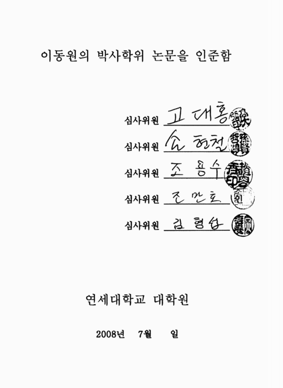
표제지
감사의 글
목차
국문요약 15
제1장 서론 18
제2장 이론적 배경 20
2.1. 소자의 스케일링(스케일일) (Scaling(Sacling)) 20
2.1.1. MOSFET의 스케일링 20
2.1.2. 실리콘산화막의 스케일링 30
2.2. 고유전박막 (high-k) 42
2.2.1. 게이트 유전막재료로서의 고려사항 42
2.2.2. ZrO₂와 HfO₂ 박막의 물리적 성질 61
제3장 ALD 법으로 성장시킨 HfO₂ 및 Hf silicate 박막의 미세구조 및 물리적 특성 71
3.1. 서론 71
3.2. 실험 74
3.2.1. 실험 장치 74
3.2.2. 실험 방법 83
3.3. ALD로 성장시킨 HfO₂와 Hf silicate 박막의 미세 구조 93
3.3.1. Hf 및 Si 전구체의 선택 93
3.3.2. ALD로 성장시킨 HfO₂ 증착 특성 97
3.3.3. ALD로 성장시킨 HfO₂ 박막의 후속 열처리에 따른 물성 변화 110
3.4. ALD로 성장시킨 Hf silicate 박막 특성연구 117
3.4.1. Hf-silicate 박막의 Si조성에 따른 물리적 특성 117
3.4.2. Hf silicate 박막의 Si조성에 따른 전기적 특성 132
3.5. 결론 140
제4장 ALD 법으로 성장시킨 Hf silicate박막의 후속 열처리에 따른 미세구조 및 물리적, 전기적 특성 연구 142
4.1. 서론 142
4.2. 실험방법 145
4.3. 후속 열처리에 따른 Hf silicate 박막의 미세구조 변화 147
4.4. 후속 열처리에 따른 Hf-ailicate 박막의 전기적 특성 변화 157
4.5. 결론 166
참고 문헌 168
ABSTRACT 186
Fig. 2-1. Moore's Law, the doubling of transistors every couple of years, has been maintained, and still holds true today. 25
Fig. 2-2. Cross-sectional view of the basic p-bulk (n-channel) MOSFET structure. 27
Fig. 2-3. Band diagram and FET. 29
Fig. 2-4. Structure of SiO₂ The 6-membered ring structure of SiO₂ is shown conceptually on the right. 34
Fig. 2-5. Model of silicon oxidation. 35
Fig. 2-6. (a) Conceptual atomic level picture of the Si/SiO₂ interface showing possible structural origins of Qf and Qit, and (b) 4 types of charges associated with the SiO₂/Si system.(이미지참조) 40
Fig. 2-7. (a) Gate leakage upon for various oxide thickness and (b) EOT as a function of physical oxide thickness. 41
Fig. 2-8. Band offset calculations for a number of potential high-k gate dielectric materials. 48
Fig. 2-9. Correlation between Eg, k, and leakage current. 49
Fig. 2-10. Ellingham Diagram for formation of metal oxide. 53
Fig. 2-11. Ternary phase diagrams for (a) Ta-Si-O, (b) Ti-Si-O, and (c) Zr-Si-O compounds. 55
Fig. 2-12. Three types of growth modes : (a) Frank-van der Merwe groth mode, (b) Volmer-Weber growth mode, and (c) Stranski-Kratanov growth mode. 66
Fig. 2-13. Leakage current at 1MV/cm and k versus temperature of post-sputtering anneal for Ta205 films. 69
Fig. 2-14. Fluorite structure and its (110) plane. 70
Fig. 3-1. A schematic diagram of the basic principle of the ALD processing. 78
Fig. 3-2. A processing window of the ALD process. 80
Fig. 3-3. Schematic view of (a) vertical furnace and (b) RTP. 81
Fig. 3-4. Rotation type spectroscopic ellipsometer. 88
Fig. 3-5. Schematic flow chart for TEM specimen preparation. 89
Fig. 3-6/3-7. Clausius-Clapeyron plots of Hf[N(CH₃)(C2H5)]₄ (TEMAHf) and Hf[N(C2H5)₂]₄ (TDEAHf). Vapor pressure of Hf[N(CH₃)(C2H5)]₄, and Hf[N(C2H5)₂]₄ are ~0.5Torr, and ~0.1 Torr at the temperature of 85℃, respectively.(이미지참조) 95
Fig. 3-7/3-8. Clausius-Clapeyron plots of SiH[N(CH₃)₂]₃, Si[N(CH₃)₂]₄, and SiH[N(C2H5)₂]₃. Vapor pressure of SiH[N(CH₃)₂]₃ are ~25 Torr at the temperature of 50℃.(이미지참조) 96
Fig. 3-8/3-9. Thickness of HfO₂ films measured by spectroscopic ellipsometer 100
Fig. 3-9/3-10. HR-TEM images of as-deosited. HfO₂ ; (a) 2 nm, (b) 3 nm, (c) 4 nm, (d) 5nm, and (e) 8nm 101
Fig. 3-10/3-11. XPS wide scan spectrum of HfO₂ and SiO₂ film 104
Fig. 3-11/3-12. C-V characterizatics upon film thickness of HfO₂ 107
Fig. 3-12/3-13. EOT of HfO₂ upon the thickness of HfO₂ increased 109
Fig. 3-13/3-14. XRD spectra of as-deposited ~8 nm thick HfO₂ at various annealing temperature 112
Fig. 3-14/3-15. HR-TEM image of ~5 nm thick HfO₂ at various annealing temperature ; (a) as~dep., (b) annealing at 600℃ and (c) at 800℃ 113
Fig. 3-15/3-16. Capacitance-Voltage Curve and C/Co of ~5 nm thick HfO₂at various annealing temperature ; (a) Capacitance-Voltage Curve, and (b) C/Co-Voltage Curve 115
Fig. 3-16/3-17. XPS wide scan spectra of various compositional Hf silicate film 120
Fig. 3-17/3-18. Cycle ratio vs. Composition of various Hf silicate films 121
Fig. 3-18/3-19. (a) Hf 4f and (b) Si 2p photoelectron spectra with various compositional Hf silicate 123
Fig. 3-19/3-20. refractive index and extinction coefficient spectra with various compositional Hf silicate measured by spectroscopic ellipsometer 125
Fig. 3-20/3-21. HR-TEM image of as-depoited HS51 ; (a) 3 nm thick. (b) 4 nm thick. (c) 5 nm thick. and (d) 8 nm thick 127
Fig. 3-21/3-22. HR-TEM image of as-depoited HS31 ; (a) 3 nm thick. (b) 4 nm thick. (c) 5 nm thick. and (d) 8 nm thick 128
Fig. 3-22/3-23. HR-TEM image of as-depoited HS11 ; (a) 3 nm thick. (b) 4 nm thick. (c) 5 nm thick. and (d) 8 nm thick 129
Fig. 3-23/3-24. HR-TEM image of as-depoited HS13 ; (a) 3 nm thick. (b) 4 nm thick. (c) 5 nm thick. and (d) 8 nm thick 130
Fig. 3-24/3-25. HR-TEM image of as-depoited HS15 ; (a) 3 nm thick. (b) 4 nm thick. (c) 5 nm thick. and (d) 8 nm thick 131
Fig. 3-25/3-26. C-V characterizatics upon composition of Hf silicate ; (a) HS51, (b) HS11, and (c) HS15 135
Fig. 3-26/3-27. EOT of various Hf silicates upon the thickness increased 136
Fig. 3-27/3-28. Dielectric constant vs. composition of Hf silicates 137
Fig. 3-28/3-29. Capacitance-voltage curve of ~5 nm thickness Hf silicates 138
Fig. 4-1. Schmatic of passible issues when high k dielectric gats stack used 144
Fig. 4-2. XRD spectra of Hf silicate with annealing temperature ; (a) HfO₂, (b) HS51, (c) HS31, (d) HS11, (e) HS13, and (f) HS15 150
Fig. 4-3. NEXAFS O k edge absorption spectra of Hf silicate with annealing temperature ; (a) HfO₂, (b) HS51, (c) HS31, (d) HS11, (e) HS13, and (f) HS15 151
Fig. 4-4. HR-TEM image of ~5 nm thick HS51 at various annealing temperature ; (a) as-dep., (b) annealing at 700℃, (c) at 800℃ and (d) at 900℃ 152
Fig. 4-5. HR-TEM image of ~5 nm thick HS11 at various annealing temperature ; (a) as-dep., (b) annealing at 600℃, (c) at 800℃ and (d) at 900℃ 153
Fig. 4-6. HR-TEM image of ~5 nm thick HS11 annealed at 900℃ ; (a) High resolution image and (b) low-magnitude image 154
Fig. 4-7. (a) Hf 4f and (b) O 1s photoelectron spectra of HS11 with annealing temperature 155
Fig. 4-8. HR-TEM image of ~5 nm thick HS15 at various annealing temperature ; (a) as-dep., (b) annealing at 700℃, (c) at 800℃ and (d) at 900℃ 156
Fig. 4-9. Capacitance-Voltage Curve of ~5 nm thick HS15 at various annealing temperature 160
Fig. 4-10. Capacitance-Voltage Curve of ~5 nm thick HS11 at various annealing temperature 162
Fig. 4-11. Capacitance-Voltage Curve of ~5 nm thick HS15 at various annealing temperature 164
| 번호 | 참고문헌 | 국회도서관 소장유무 |
|---|---|---|
| 1 | The electronic structure at the atomic scale of ultrathin gate oxides  |
미소장 |
| 2 | Evaluating the minimum thickness of gate oxide on silicon using first-principles method |
미소장 |
| 3 | Gate oxides in 50 nm devices: thickness uniformity improves projected reliability |
미소장 |
| 4 | Ultimate limit for defect generation in ultra-thin silicon dioxide |
미소장 |
| 5 | "Boron diffusion and penetration in ultrathin oxide with poly-Si gate", IEEE Electron Device Lett. 1 9, 291 (1998) | 미소장 |
| 6 | Effects of Gate Depletion and Boron Penetration on Matching of Deep Submicron CMOS Transistors |
미소장 |
| 7 | Gate Quality Doped High K Films for CMOS Beyond 100nm: 3-10nm AlO with Low Leakage and Low Interface States |
미소장 |
| 8 | High-resolution depth profiling in ultrathin Al2O3 films on Si |
미소장 |
| 9 | "High quality La2O3 and Al2O3 gate dielectrics with equivalent oxide thickness 5-10Å", Tech. Dig. VLSI Symp. 2000, p. 16. | 미소장 |
| 10 | "Characteristics of Al2O3 gate dielectric prepared by atomic layer deposition for giga scale CMOS DRAM devices", Tech. Dig. VLSI Symp. 2000, p.46. | 미소장 |
| 11 | "Effect of polysilicon gate on the flatband voltage shift and mobility degradation for ALD-Al2O3 gate dielectric ", Tech. Dig. Int. Electron Devices Meet. 2000, p. 645. | 미소장 |
| 12 | Atomic beam deposition of lanthanum- and yttrium-based oxide thin films for gate dielectrics |
미소장 |
| 13 | Interfacial reactions in the thin film Y 2O 3 on chemically oxidized Si(100) substrate systems |
미소장 |
| 14 | Temperature dependence of the properties of heteroepitaxial Y2O3 films grown on Si by ion assisted evaporation |
미소장 |
| 15 | High ε gate dielectrics Gd2O3 and Y2O3 for silicon |
미소장 |
| 16 | Atomic beam deposition of lanthanum- and yttrium-based oxide thin films for gate dielectrics |
미소장 |
| 17 | "Epitaxial praseodymium oxide: a new high-k dielectric", Tech. Dig. Int. Electron Devices Meet. 2000, p. 653. | 미소장 |
| 18 | Does Chemistry Really Matter in the Chemical Vapor Deposition of Titanium Dioxide? Precursor and Kinetic Effects on the Microstructure of Polycrystalline Films |
미소장 |
| 19 | "Zirconium oxide based gate dielectrics with equivalent oxide thickness of less than 1.0 nm and performance of submicron MOSFET using a nitride gate replacement process", Mater. Res. Soc. Symp. Proc. 5 67, 355 (1999). | 미소장 |
| 20 | "Sub-quarter micron CMOS process for TiN-gate MOSFETs with TiO2 gate dielectric formed by titanium oxidation", Tech. Dig. VLSI Symp. 1999, p. 133. | 미소장 |
| 21 | "MOSCAP and MOSFET characteristics using ZrO2 gate dielectric deposited directly on Si ", IEEE Trans. Electron Devices ED-33 , 442 (1986). | 미소장 |
| 22 | MOSCAP and MOSFET Characteristics Using ZrO~2 Gate Dielectric Deposited Directly on Si |
미소장 |
| 23 | "MOS characteristics of ultra thin rapid thermal CVD ZrO2 and Zr silicate gate dielectrics " Tech. Dig. Int. Electron Devices Meet. 2000, p. 27. | 미소장 |
| 24 | Low Temperature Chemical Vapor Deposition of ZrO[sub 2] on Si(100) Using Anhydrous Zirconium (IV) Nitrate |
미소장 |
| 25 | A β-1,3-glucan binding protein from the black tiger shrimp, Penaeus monodon |
미소장 |
| 26 | Thermal decomposition of ZrO2/SiO2 bilayer on Si(001) caused by void nucleation and its lateral growth |
미소장 |
| 27 | Thermal stability and electrical characteristics of ultrathin hafnium oxide gate dielectric reoxidized with rapid thermal annealing |
미소장 |
| 28 | "Electrical characteristics of highly reliable ultrathin hafnium oxide gate dielectric", IEEE Electron Device Lett. 2 1, 181 (2000). | 미소장 |
| 29 | "High quality ultra thin CVD HfO2 gate stack with poly-Si gate electrode", Tech. Dig. Int. Electron Devices Meet. 2000, p. 31. | 미소장 |
| 30 | Influence of annealing condition on the properties of sputtered hafnium oxide |
미소장 |
| 31 | Dielectric property and thermal stability of HfO2 on silicon |
미소장 |
| 32 | CMOS Metal Replacement Gate Transistors Using Tantalum Pentoxide Gate Insulator |
미소장 |
| 33 | Stacked high-ε gate dielectric for gigascale integration of metal–oxide–semiconductor technologies |
미소장 |
| 34 | "MOS transistors with stacked SiO2-Ta2O5-SiO2 gate dielectrics for giga-scale integration of CMOS technologies", IEEE Electron Device Lett. 1 9, 423 (1998). | 미소장 |
| 35 | Crystalline Oxides on Silicon - Alternative Dielectrics for Advanced Transistor Technologies |
미소장 |
| 36 | Properties of Epitaxial SrTiO~3 Thin Films Grown on Silicon by Molecular Beam Epitaxy |
미소장 |
| 37 | Ion Transport Phenomena in Insulating Films |
미소장 |
| 38 | Metal-nitride-oxide-silicon field-effect transistors, with self-aligned gates |
미소장 |
| 39 | Silicon gate technology |
미소장 |
| 40 | "Design and Characteristics of the Lightly Doped Drain-Source(LDD) Insulated Gate Field-Effect Transistor". IEEE Trans. Ed-27, 1359 (1980). | 미소장 |
| 41 | "Cramming More Components Onto Integrated Circuits," Electronics Magazine. 8, 114 (1965). | 미소장 |
| 42 | See The International Technology Roadmap for Semiconductors, Semiconductor Industry Association; see also http: //public.itrs.net/ for the most recent updates (1999). | 미소장 |
| 43 | Submicron short channel effects due to gate reoxidation induced lateral interstitial diffusion |
미소장 |
| 44 | "Design Of Ion-implanted MOSFET's with Very Small Physical Dimensions", IEEE J. SC-9, 256 (1974). | 미소장 |
| 45 | "Generalized Scaling Theory and Its Application to a 1/4 Micrometer MOSFET Design". IEEE Trans. ED-31 , 452 (1984). | 미소장 |
| 46 | Gate Dielectrics and MOS ULSIs (Springer, New York, 1997). | 미소장 |
| 47 | IEEE Trans. Electron Device, ED-1 2, p.97, 1965. | 미소장 |
| 48 | General Relationship for the Thermal Oxidation of Silicon |
미소장 |
| 49 | SILICON VLSI TECHNOLOGY (Prentice Hall, New Jersey, 2000). | 미소장 |
| 50 | A high‐resolution electron microscopy study of the Si‐SiO 2 interface |
미소장 |
| 51 | Model for Radiation‐Induced Charge Trapping and Annealing in the Oxide Layer of MOS Devices |
미소장 |
| 52 | Oxide thickness dependence of electron‐induced surface states in MOS structures |
미소장 |
| 53 | "Standardized Terminology for Oxide Charges Associated with Thermally Oxidized Silicon". IEEE Trans. Elec. Dev., vol. ED-27, p. 606, (1980). | 미소장 |
| 54 | Electronic Properties of the Si/SiO~2 Interface from First Principles |
미소장 |
| 55 | Low Leakage, Ultra-Thin Gate Oxides for Extremely High Performance sub-100nm nMOSFETs |
미소장 |
| 56 | Progress Toward 10nm CMOS Devices |
미소장 |
| 57 | The Ballistic Nano-Transistor |
미소장 |
| 58 | "Ultra thin gate SiO2 technology". Proc.-Electrochem. Soc. 2000-2, p. 3. | 미소장 |
| 59 | "Limits of gateoxide scaling in nano-transistors", VLSI Tech. Dig. 2000, p. 90. | 미소장 |
| 60 | Tech. Dig. VLSI Symp. 2000, p. 174; R. R. Chau, J. Kavalieros, B. Roberds, R. Schenker, D. Lionberger, D. Barlage, B. Doyle, R. Arghavani, A. Murthy, and G. Dewey, "Scaling challenges and device design requirements for high performance sub-50 nm gate length planar CMOS transistors", Tech. Int. Electron Devices Meet. 2000, p. 45. | 미소장 |
| 61 | Minimization of Interfacial Microroughness for 13 - 60 � Ultrathin Gate Oxides |
미소장 |
| 62 | In situ Si flux cleaning technique for producing atomically flat Si(100) surfaces at low temperature |
미소장 |
| 63 | "Quantum mechanical modeling of electron tunneling current from the inversion layer of ultra-thinoxide nMOSFET's " IEEE Electron Device Letter, 1997, p. 209. | 미소장 |
| 64 | Principles of Electrical Engineering Materials and Devices, 2nd Ed. (McGraw-Hill, New York, 2002). | 미소장 |
| 65 | INTRODUCTION TO CERAMICS, 2nd Ed. (John Wiely & Sons, Singapore, 1991). | 미소장 |
| 66 | Dielectric polarizabilities of ions in oxides and fluorides |
미소장 |
| 67 | Physics of Semiconductor Devices, 2nd ed.(Wiley, New York, 1981). | 미소장 |
| 68 | New York: The Politics of Urban Regional Development by Michael N. Danielson; |
미소장 |
| 69 | Schottky barrier heights of tantalum oxide, barium strontium titanate, lead titanate, and strontium bismuth tantalate |
미소장 |
| 70 | Band offsets of wide-band-gap oxides and implications for future electronic devices |
미소장 |
| 71 | Circuit Requirement and Integration Challenges of Thin Gate Dielectrics for Ultra Small MOSFETs |
미소장 |
| 72 | Thermodynamic considerations in refractory metal‐silicon‐oxygen systems |
미소장 |
| 73 | Res |
미소장 |
| 74 | Reactions of Zr thin films with SiO 2 substrates |
미소장 |
| 75 | Thermodynamics in materials science (McGraw-Hill, Singapore, 1993) | 미소장 |
| 76 | Thermochemical Properties of Inorganic Substances (Springer, Berlin, 1973). | 미소장 |
| 77 | Thermodynamic Properties of Elements and Oxides (U.S. Dept. of Interior, Bureau of Mines Bulletin 672, U.S. Govt. Printing Office, Washington, D.C., 1982). | 미소장 |
| 78 | Silicides for VLSI Applications (Academic, New York, 1983). | 미소장 |
| 79 | Void formation on ultrathin thermal silicon oxide films on the Si(100) surface |
미소장 |
| 80 | Bonding constraints and defect formation at interfaces between crystalline silicon and advanced single layer and composite gate dielectrics |
미소장 |
| 81 | "Effect of Oxide Defect Structure on the Electrical Properties of ZrO2". J. Am. Chem. Soc. 55, 439 (1972). | 미소장 |
| 82 | Low Temperature Chemical Vapor Deposition of ZrO[sub 2] on Si(100) Using Anhydrous Zirconium (IV) Nitrate |
미소장 |
| 83 | Hafnium and zirconium silicates for advanced gate dielectrics |
미소장 |
| 84 | "80 nm polysilicon gated n-FETs with ultra-thin Al2O3 gate dielectric for ULSI applications ", Tech. Dig. Int. Electron Devices Meet. 2000, p. 223. | 미소장 |
| 85 | CMOS Metal Replacement Gate Transistors Using Tantalum Pentoxide Gate Insulator |
미소장 |
| 86 | Zirconium Oxide Based Gate Dielectrics with Equivalent Oxide Thickness of Less Than 1.0nm and Performance of Submicron MOSFET using a Nitride Gate Replacement Process |
미소장 |
| 87 | "Electrical properties of heavily doped polycrystalline silicon-germanium films", IEEE Trans. Electron Devices 41, 228 (1994). | 미소장 |
| 88 | "Highly reliable poly-SiGe/amorphous-Si gate CMOS", Tech. Dig. Int. Electron Devices Meet. 2000, p.445. | 미소장 |
| 89 | Variation in the fixed charge density of SiO[sub x]/ZrO[sub 2] gate dielectric stacks during postdeposition oxidation |
미소장 |
| 90 | Structure and stability of ultrathin zirconium oxide layers on Si(001) |
미소장 |
| 91 | Crystalline zirconia oxide on silicon as alternative gate dielectrics |
미소장 |
| 92 | Amorphous lanthanide-doped TiOx dielectric films |
미소장 |
| 93 | Field effect transistors with SrTiO3 gate dielectric on Si |
미소장 |
| 94 | Properties of Epitaxial SrTiO~3 Thin Films Grown on Silicon by Molecular Beam Epitaxy |
미소장 |
| 95 | (ed.), Binary Alloy Phase Diagrams (V.1.Materials Park, Ohio:ASM International, 1990). | 미소장 |
| 96 | Mechanisms for success or failure of diffusion barriers between aluminum and silicon |
미소장 |
| 97 | Metal/metal‐oxide interfaces: A surface science approach to the study of adhesion |
미소장 |
| 98 | Prediction of phase formation sequence and phase stability in binary metal‐aluminum thin‐film systems using the effective heat of formation rule |
미소장 |
| 99 | Thin film Phenomenon (Robert E. Krieger Publishing Company, Malabar, Fla., 1985). | 미소장 |
| 100 | 엔지니어링 세라믹스 (반도 출판사, 1990). | 미소장 |
| 101 | Influence of substrate temperature on atomic layer growth and properties of HfO 2 thin films |
미소장 |
| 102 | "Crystal Structure and Equation of State of Cotunnite-Type Zirconia". J. Am. Ceram. Soc. 78, 445 (1995) | 미소장 |
| 103 | "High-density ZrO2 and HfO2: Crystalline structures and equations of state", Phys. Rev. B 5 9, 8467 (1999). | 미소장 |
| 104 | Exchange-biasing mechanism in La 2 / 3 Ca 1 / 3 MnO 3 / La 1 / 3 Ca 2 / 3 MnO 3 multilayers |
미소장 |
| 105 | Growth and structure control of HfO2−x films with cubic and tetragonal structures obtained by ion beam assisted deposition |
미소장 |
| 106 | "High temperature stability in lanthanum and zirconia-based gate dielectrics", J. Appl. Phys. 9 0, 3476 (2000). | 미소장 |
| 107 | "Oxygen exchange and transport in thin zirconia films on Si(100)", Phys. Rev. B 6 2, 290 (2000). | 미소장 |
| 108 | Thermal stability of ultrathin ZrO2 films prepared by chemical vapor deposition on Si(100) |
미소장 |
| 109 | Advanced Inorganic Chemistry (Wiley, New York, 2000). | 미소장 |
| 110 | Thermodynamic stability of high- K dielectric metal oxides ZrO2 and HfO2 in contact with Si and SiO2 |
미소장 |
| 111 | "Special points for Brillouin-zone integrations", Phys. Rev. B 13 , 5188 (1976). | 미소장 |
| 112 | Thermodynamic Data of Pure Substances, 3rd ed. (VCH, Weinheim, 1995). | 미소장 |
| 113 | Ed., VLSI Technology, 2nd ed. (McGraw Hill, New York, (1988). | 미소장 |
| 114 | Appl. Phys. Lett. 82, 106 (2003). | 미소장 |
| 115 | Electorchem. Solid-State Lett. 8, F51 (2005). | 미소장 |
| 116 | J. Appl. Phys. 97, 124107 (2005). | 미소장 |
| 117 | Solid State Technol. 46, 45 (2003). | 미소장 |
| 118 | Appl. Phys. Lett. 85, 5953 (2004). | 미소장 |
| 119 | Electorchem. Solid-State Lett. 7, F42 (2004). | 미소장 |
| 120 | Electrochem. Solid-State Lett. 8, G215 (2005). | 미소장 |
| 121 | Introduction to Ceramics, 2nd Edition (Wiley, New York, 1976). | 미소장 |
| 122 | Accepted to Appl. Phys. Lett. (2004). | 미소장 |
| 123 | Appl. Phys. Lett. 82, 106 (2003). | 미소장 |
| 124 | Introduction to Solid State Physics (Wiley, New York, 1986), p 370 | 미소장 |
| 125 | Appl. Phys. Lett. 77, 2912 (2000). | 미소장 |
| 126 | Tech. Dig. Int. Electron Devices Meet. 2003, 797 (2003). | 미소장 |
*표시는 필수 입력사항입니다.
| 전화번호 |
|---|
| 기사명 | 저자명 | 페이지 | 원문 | 기사목차 |
|---|
| 번호 | 발행일자 | 권호명 | 제본정보 | 자료실 | 원문 | 신청 페이지 |
|---|
도서위치안내: / 서가번호:

우편복사 목록담기를 완료하였습니다.
*표시는 필수 입력사항입니다.
저장 되었습니다.
