권호기사보기
| 기사명 | 저자명 | 페이지 | 원문 | 기사목차 |
|---|
| 대표형(전거형, Authority) | 생물정보 | 이형(異形, Variant) | 소속 | 직위 | 직업 | 활동분야 | 주기 | 서지 | |
|---|---|---|---|---|---|---|---|---|---|
| 연구/단체명을 입력해주세요. | |||||||||
|
|
|
|
|
|
* 주제를 선택하시면 검색 상세로 이동합니다.
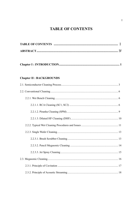
Title Page
Contents
ABSTRACT 7
Chapter I. INTRODUCTION 9
1. Introduction 9
Chapter II. BACKGROUND 11
2.1. Semiconductor Cleaning Process 11
2.2. Conventional Cleaning 14
2.2.1. Wet Bench Cleaning 14
2.2.2. Wet Bench Cleaning Procedures and Issues 19
2.2.3. Single Wafer Cleaning 21
2.3. Megasonic Cleaning 24
2.3.1. Principle of Cavitation 25
2.3.2. Principle of Acoustic Streaming 27
2.4. Issues in Nano Particle Removal 29
Chapter III. EXPERIMENTAL MATERIALS AND PROCEDURES 31
3.1. Experimental Materials 31
3.2. Characterization Methods 32
3.2.1. Spectroscopic Ellipsometer 32
3.2.2. Surface Particle Scanner 34
3.2.3. Sound Pressure Measurement 36
3.2.4. Gas Concentration Measurement 38
3.3. Experimental Procedure 40
3.3.1. Particle Deposition 40
3.3.2. DIW Aeration for Gas Injection 41
3.3.3 Rod Type Single Wafer Megasonic System 43
Chapter IV. RESULTS AND DISCUSSIONS 45
4.1. Generation of Cavitation 45
4.1.1. Bubble image on Wafer using Aerator DIW 45
4.1.2. Effect of Aerator at DIW, Hot DIW and SC1 47
4.2. Fundamental Evaluation of Bar Type Megasonic System 51
4.2.1. Effect of Wafer Q-Time 51
4.2.2. Effect of Gap between wafer and rod 52
4.2.3. Effect of Wafer rpm 53
4.2.4. Effect of Megasonic radiation Power 55
4.2.5. Effect of Megasonic Radiation Time 56
4.3. Bar Type Megasonic System on Chemicals 57
4.3.1. Effect of Chemicals 57
4.3.2. Effect of Temp of Chemicals. 58
4.4. Sound Pressure and Particle Removal Efficiency 59
4.4.1. Effect of wide range Frequency (by MHz) Variation 59
4.4.2. Effect of narrow range Frequency (by KHz) Variation 61
4.4.3. Effect of Megasonic Power 63
4.5. Nano-Particle Removal Efficiency 65
4.5.1. Effect of Cleaning Chemical with Megasonic 65
4.5.2. Effect of Megasonic Power 66
4.5.3. Effect of Megasonic Frequency 67
4.5.4. Effect of HF additional treatment 68
4.6. Etching Amount by Chemicals 69
Chapter V. SUMMARY AND CONCLUSION 70
Chapter VI. REFERENCES 72
국문요지 76
감사의 글 78
Figure 2.1. Semiconductor fabrication processes 12
Figure 2.2. Cross Section Image of 65nm Logic Device 12
Figure 2.3. A schematic diagram of particle removal mechanism using SC1 solution 15
Figure 2.4. RCA cleaning and Beyond [2.5] 16
Figure 2.3. Typical wet cleaning tool configurations. 19
Figure 2.4. Suggested Roadmap toward cleans with lower chemical and DIW consumption [2.10]. 20
Figure 2.5. Brush Mark after Cleaning (>65nm particle Size) 21
Figure 2.6. (a) Image of Pencil Megasonic Cleaning systems, and (b) pattern damaged picture. 22
Figure 2.7. Image of Jet Spray Cleaning systems 23
Figure 2.8. Transient Cavitation thresholds 24
Figure 2.9. Bubble implosion sequence by acoustic streaming [2.14] 26
Figure 2.10. Bubble generation and shock wave emission upon laser-induced breakdown caused by a focused Nd:YAG laser pulse in water. [2.15] 26
Figure 2.11. Schematic diagram of the acoustic microstreaming sequence [2.17] 28
Figure 3.1. Schematics of Spectroscopic Ellipsometer 33
Figure 3.2. Analog scatter signals versus time for 0.120μm PSL Spheres 35
Figure 3.3. Hydrophone checking Image on the wafer 37
Figure 3.4. Schematic diagram and Assembly of Aerator System. 42
Figure 3.5. Image of Bar Type Megasonic System and Megasonic Generation 44
Figure 4.1. Still Image of Degassed DIW with Megasonic 46
Figure 4.2. Still Images of Gasified DIW with Megasonic and Spinning Wafer 46
Figure 4.3. Particle Removal Efficiency by N₂ and O₂ Concentration Ratio respectively. 47
Figure 4.4. N2 Concentrations in DIW by N2 Supplying Pressure. 48
Figure 4.5. Particle Removal Efficiency by changing N₂ and O₂ Concentration. 49
Figure 4.6. Particle Removal Efficiency of SC1, HDIW by N₂ Concentration. 50
Figure 4.7. Particle Removal Efficiency Aging Wafer on FOUP 51
Figure 4.8. Particle Removal Efficiency Changing Wafer Gap 52
Figure 4.9. Effect of Wafer Spin Speed on Particle Removal Efficiency 53
Figure 4.10. Particle Wafer Images after DIW Meg (Ambient) for 30sec with 30Watt 54
Figure 4.11. Particle Removal Efficiency by Megasonic Power 55
Figure 4.12. Particle Removal Efficiency as a function of Megasonic irritation Times 56
Figure 4.13. Particle Removal Efficiency of Chemicals 57
Figure 4.14. Particle Removal Efficiency as function of temperature of Chemicals. 58
Figure 4.15. Sound Pressures and Particle Removal Efficiency by Meg Frequency has large Variation 60
Figure 4.16. Sound Pressures and Particle Removal Efficiency by Meg Frequency small Variation 62
Figure 4.17. Sound Pressures by Megasoinc Power Variation on 3kinds of Rods. 64
Figure 4.18. PRE comparisons of chemicals. 65
Figure 4.19. Size effect on PRE with Megasonic Frequency 67
Figure 4.20. Effect of Layer surface and HF treatment with SC1 Megasonic 68
Figure 4.21. Etching Amount of Layers at different Chemical conditions 69
1970년대 W. Kern이 RCA 세정 방법을 발표한 이후로, SC1은 반도체 Fab. 공정에서 Si Wafer 세정을 위하여 Wet Bench 설비를 이용하여 넓고 유용하게 사용되고 있다. SC1의 세정력이 아무리 좋다 하더라도 Wet Bench 설비에서는 공정의 한계에 다다르고 있다. IC 디바이드의 조밀도 증가와 면적 축소화 경향은 반도체 디바이스에 있어서 세정 공정의 식각량 (수 옹스트롱 이내) 감소와 수십 나노 마이크로의 Particle 제거를 요구하고 있다. 전통적인 RCA 세정은자체 한계에 다다르고 있다. IC 디바이스의 요구 조건에 만족하려고 하면, 첫번째로 세정공정은 초 희석 세정액을 사용하여야 하고, 두 번째로 Particle 제거 효율을 향상시키기 위하여 어떤 새로운 기술이 개발되어야 한다. 이러한 요구에 만족하기 위하여, 최근에 싱글 Wafer 세정 설비가 발표되고 있다. 이것들에는 여러 가지 기술이 있는데, Pencil Megasonic, Brush Scrubber, N2 가압 Jet Spray, Rod형 Megasonic, Hot-DIW Vapor Spray, 싱글 Panel Megasonic 등이다. 이것들 중에서 Bar Type Megasonic은 IC 디바이스의 요구에 만족할 수 있는 공정 능력을 갖추고 있다. 이것은 초 희석 세정액을 사용함에도 세정효율이 매우 높으며, 이에 따른 식각량도 매우 낮다. 약한 Energy의 Megasonic가 세정액과 함께 사용된다. 또한 이것은 Wafer의 경면과 이면의 Particle 동시에 제거할 수 있다.
이 논문에서는 싱글 Wafer세정설비인 Bar Type Megasonic의 특성에 대하여 연구하고, Megasonic 세정 능력 향상을 위하여 DIW와 세정액에 공기를 어떻게 넣을 것인지, Megasonic 세정 효율은 어떠한지, Megasonic Energy 밀도는 어떠한지, 어떻게 하면 여러 막질의 PRE를 향상시킬 수 있는지를 연구하였다.
DIW (N₂ & O₂ < 1ppm) Megasonic 세정은 65nm이상의 Particle에서 10%미만의 매우 낮은 PRE를 보여주고 있지만, Aerator를 이용하여 N₂ 압력을 7psi로 높여 DIW의 N₂ 농도를 25ppm까지 올린 결과, PRE는 급격한 상승을 하여 40%에 다다랐다. 이 Megasonic 설비의 최적 조건은 Wafer와 Rod의 Gap이 2.2mm, Wafer 회전수 18 ~ 24 rpm 이다. Silicon Wafer와 산화막질 Wafer에서 65nm Silicon Nitride particle 제거력은 SC1(65℃ 30sec ≥30Watt power) 조건에서 95%였다. 하지만, 질화막질 위에서 PRE가 65% 였지만, 희석 HF 5초 처리를 SC1 Megasonic전에 한 결과, PRE는 95% 향상 되었다.
100 나노 이하의 Particle 제거력은 순수 DIW만을 사용한 경우에는 매우 낮은 15%의 제거력 분포를 보이지만, 알카리계 세정액을 사용함에 따라 35%로 비율이 높아진다. 하지만, Megasonic Power와 Frequency 변동에 의해서는 100 나노 이하 Particle 제거력에 큰 변화가 없었다.
실험된 NC2와 SC1 용액에서 모든 막질의 식각량은 Megasonic 70W가 부여된 것과 관계없이 0.5Å미만의 결과를 보여주었고, HF를 추가 적용한 경우에는 1Å 내외의 식각량을 나타내었다. 따라서 식각량에 민감한 Device Step은 선택적으로 HF를 사용할 필요성이 있다
*표시는 필수 입력사항입니다.
| 전화번호 |
|---|
| 기사명 | 저자명 | 페이지 | 원문 | 기사목차 |
|---|
| 번호 | 발행일자 | 권호명 | 제본정보 | 자료실 | 원문 | 신청 페이지 |
|---|
도서위치안내: / 서가번호:

우편복사 목록담기를 완료하였습니다.
*표시는 필수 입력사항입니다.
저장 되었습니다.
