
 대표어
대표어


권호기사보기
| 기사명 | 저자명 | 페이지 | 원문 | 기사목차 |
|---|
결과 내 검색
동의어 포함
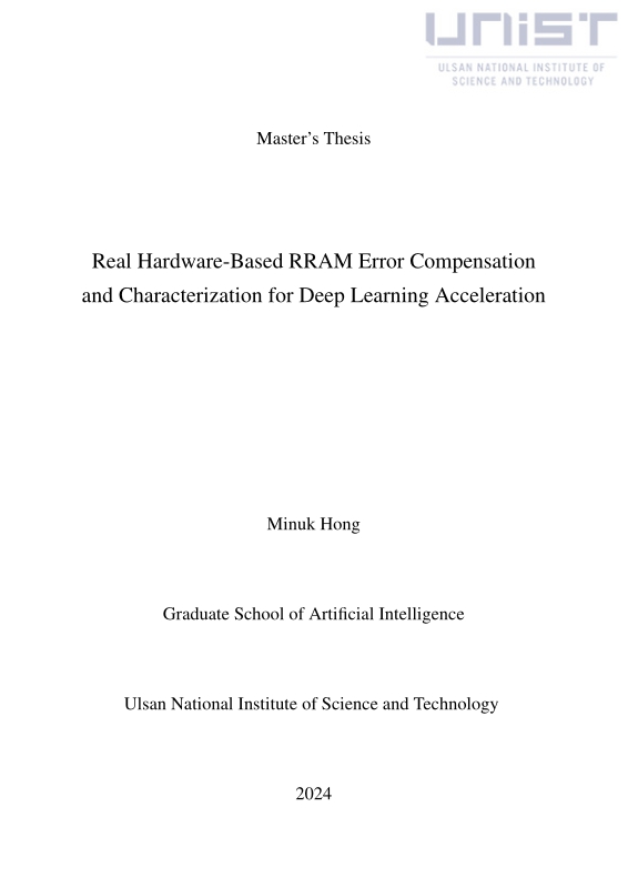
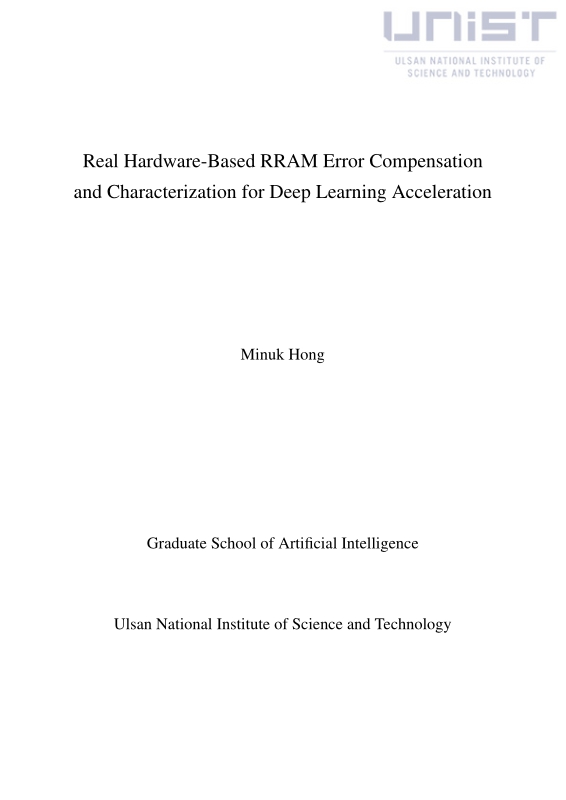
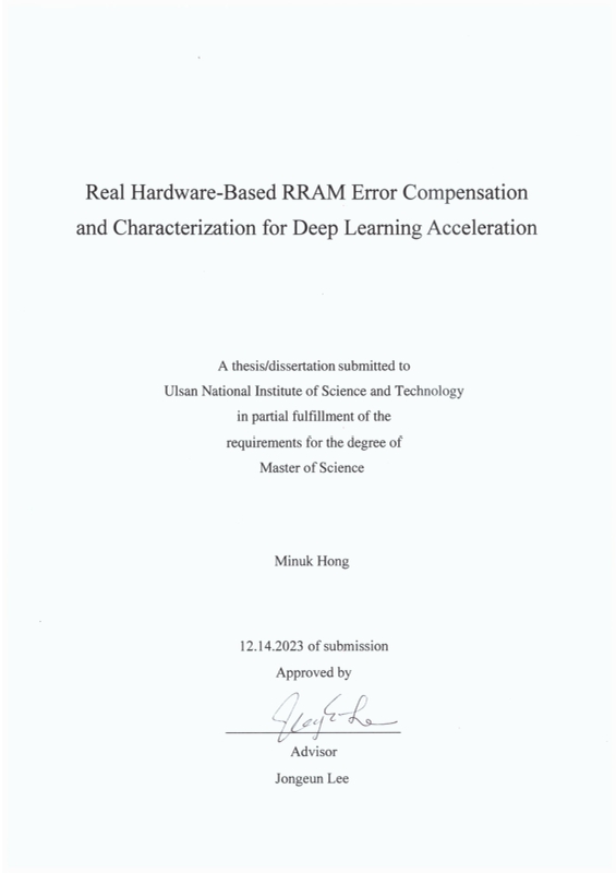
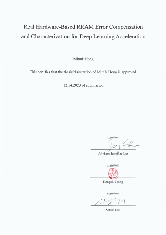
Title Page
Abstract
Contents
Ⅰ. Introduction 11
Ⅱ. Related Work 12
2.1. RRAM Variability 12
2.2. RRAM Crossbar Array Modeling Form 12
2.3. Charaterizing MVM Accuracy with Real Hardware 12
2.4. Considering Peripheral Circuit 13
Ⅲ. Background 14
3.1. Neuromorphic Computing 14
3.2. Emerging Synaptic Devices 14
3.3. Programming RCA 15
3.4. Write and Verify Scheme 15
Ⅳ. MVM Error Problem 17
4.1. Architecture 17
4.2. Procedure 17
4.3. Observation 17
Ⅴ. Analysis of MVM Error Problem 19
5.1. DAC Offset and Programming Error 19
5.2. Finding DAC Offset 20
Ⅵ. Our Proposed Method 22
6.1. Target Adjustment 22
6.2. MVM Model Adjustment 22
6.3. Comparison between TA and MA 23
Ⅶ. Characterization of MVM Accuracy with Real RRAM 26
Ⅷ. Experiments 27
8.1. Experimental Setup and Data 27
8.2. 0T1R RRAM Array HW 27
8.3. MVM Accuracy 30
8.4. Accuracy of RCA Modeling Including Programming 30
8.5. DNN Inference Results 33
Ⅸ. Conclusion 34
References 35
Figure 1. (a) von-Neumann architecture (b) Neuro-inspired Architecture. 14
Figure 2. (a) 1T1R RCA structure, (b) 0T1R RCA structure with Vdd/2 programming scheme. 16
Figure 3. Programming a cell in a passive RCA using the write-verify scheme. 16
Figure 4. Experimental MVM result degradation from the real RRAM (Ideal: ideal case, naïve: without adjustment, TA: target adjustment, MA: model adjustment). 18
Figure 5. Verify and MVM read operation for 0T1R and 1T1R. 19
Figure 6. Offset current (when input is 0) vs. read current (when input is 1), measured on a cell while changing its resistance via programming pulses. 21
Figure 7. Single column example illustrating the effect of DAC offset during MVM. 24
Figure 8. Hardware compensation implementing the MVM Model Adjustment method ("Reg"s hold the pre-computed I off value for each column). 25
Figure 9. Flow for characterization of real RRAM variability. 26
Figure 10. Heatmap resulting from single read in a 32x32 RRAM. The output of the heatmap corresponds to digital values in the conductance domain, originating from a 12-bit ADC. 27
Figure 11. (a) 8x8 Programmed matrix (b) Input activation and MVM result from 8x8 matrix. 28
Figure 12. The RRAM structure is organized with stack information on the left, and on the right, there is a printed circuit board specifically designed for RRAM wire-bonding. 28
Figure 13. Our experimental setup consisting of a RRAM chip, a peripheral PCB board, FMC connector for connecting between FPGA and PCB board, and an FPGA board which is Zedboard connected to a PC. 29
Figure 14. Experimental MVM result degradation from the real RRAM (naïve: without adjustment, TA: target adjustment, MA: model adjustment). 30
Figure 15. RMSE of variabiliy modeling between ideal MVM. 31
Figure 16. Histogram of MVM result between a 8×8 weight matrix and 2 8 different input activations (a) generated using our variability modeling (σ=0.055), (b) obtained from real RCA hardware. 32
Figure 17. Histogram of result obtained by subtracting MVM result between an 8x8 weight matrix and 2 8 different input activations from ideal MVM (a) generated using our variability modeling (σ=0.055),... 32
Figure 18. Network accuracy result of varying variability and RCA size. 33
*표시는 필수 입력사항입니다.
| 전화번호 |
|---|
| 기사명 | 저자명 | 페이지 | 원문 | 기사목차 |
|---|
| 번호 | 발행일자 | 권호명 | 제본정보 | 자료실 | 원문 | 신청 페이지 |
|---|
도서위치안내: / 서가번호:

우편복사 목록담기를 완료하였습니다.
*표시는 필수 입력사항입니다.
저장 되었습니다.
