
 대표어
대표어
 한국학술지인용색인(NRF)


권호기사보기
| 기사명 | 저자명 | 페이지 | 원문 | 기사목차 |
|---|
결과 내 검색
동의어 포함
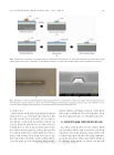
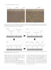
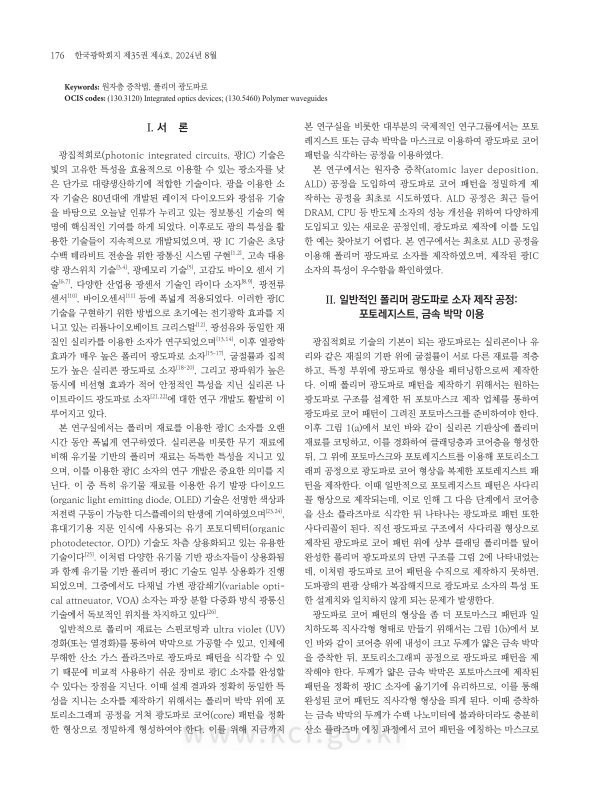
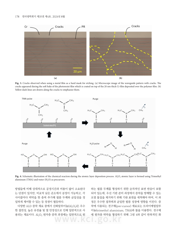
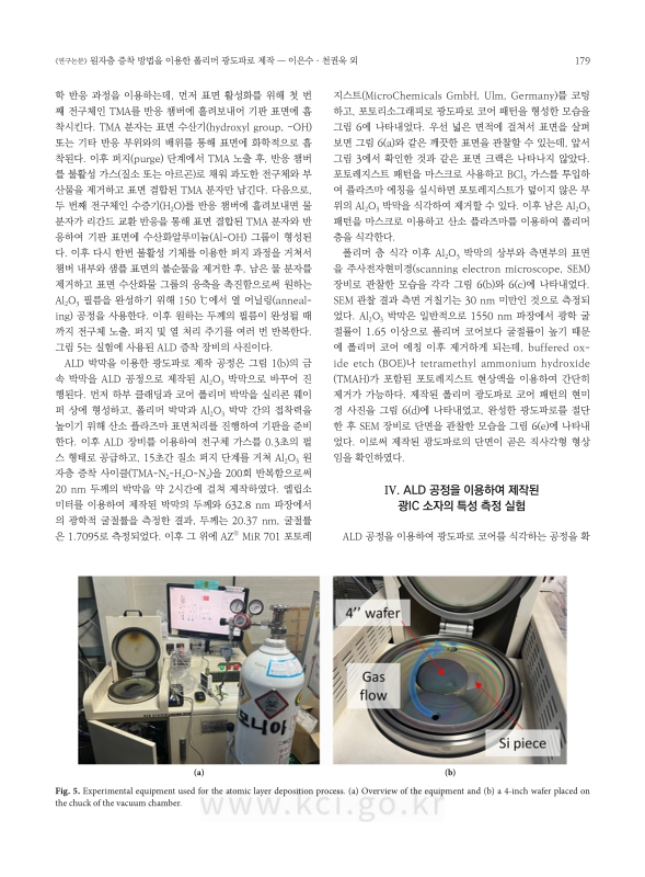
근래 광통신, 광센서, 양자광학 등의 다양한 연구 분야에서 광IC 소자를 이용한 광신호 처리 연구가 활발히 진행되고 있으며, 광IC 제작에 이용되는 재료들 중 특히 폴리머 재료는 고유의 특징을 바탕으로 폭넓게 연구개발되고 있다. 폴리머 기반 광IC 소자를 제작하기 위해서는 광도파로 단면 구조를 정확히 제작하기 위한 제작 공정을 확립하는 것이 중요하며, 특히 안정적인 소자 특성을 유지하고 대량생산 시의 수율을 높이기 위해서는 재현성이 높고 오차 수용 범위가 넓은 공정과 제작 조건을 설정하는 것이 필요하다. 본 연구에서는 원자층 증착(atomic layer deposition, ALD) 공정을 도입하여 폴리머 광도파로 소자를 효율적으로 제작할 수 있는 방법을 제안하였으며, 기존의 포토 레지스트나 금속 박막 증착을 이용하는 방법에 비해 광도파로 코어 형상을 더욱 정밀하게 제작할 수 있음을 확인하였다. 본 연구에서는 ALD 공정을 도입하여 코어의 크기가 1.8 × 1.6 µm²인 폴리이미드 광도파로를 제작하여 광도파로의 손실을 측정하고, 이와 함께 광파워 분배기인 다중모드 간섭(multi-mode interference) 광도파로 소자를 제작하여 특성을 측정하였다. 이때 기존의 제작과정에서 문제시되었던 에칭 마스크 층의 크랙 현상은 나타나지 않았으며, 광도파로 패턴 단면의 수직성도 우수하였고, 도파로의 전파손실 또한 1.5 dB/cm 이하로 양호하였다. 이로써 ALD 공정이 대량생산을 위한 폴리머 광소자 제작 공정에 적합한 방법임을 확인하였다.
Research into optical signal processing using photonic integrated circuits (PICs) has been actively pursued in various fields, including optical communication, optical sensors, and quantum optics. Among the materials used in PIC fabrication, polymers have attracted significant interest due to their unique characteristics. To fabricate polymer-based PICs, establishing an accurate manufacturing process for the cross-sectional structure of an optical waveguide is crucial. For stable device performance and high yield in mass production, a process with high reproducibility and a wide tolerance for variation is necessary. This study proposes an efficient method for fabricating polymer optical-waveguide devices by introducing the atomic layer deposition (ALD) process. Compared to conventional photoresist or metal-film deposition methods, the ALD process enables more precise fabrication of the optical waveguide’s core structure. Polyimide optical waveguides with a core size of 1.8 × 1.6 μm2 are fabricated using the ALD process, and their propagation losses are measured. Additionally, a multimode interference (MMI) optical-waveguide power-splitter device is fabricated and characterized. Throughout the fabrication, no cracking issues are observed in the etching-mask layer, the vertical profiles of the waveguide patterns are excellent, and the propagation loss is below 1.5 dB/cm. These results confirm that the ALD process is a suitable method for the mass production of high-quality polymer photonic devices.| 번호 | 참고문헌 | 국회도서관 소장유무 |
|---|---|---|
| 1 | Z. Xuan and F. Aflatouni, “Integrated coherent optical receiver with feed-forward carrier recovery,” Opt. Express 28, 16073-16088 (2020). | 미소장 |
| 2 | L. A. Valenzuela, Y. Xia, A. Maharry, H. Andrade, C. L. Schow, and J. F. Buckwalter, “A 50-GBaud QPSK optical receiver with a phase/frequency detector for energy-efficient intra-data center interconnects,” IEEE Open J. Solid-State Circuits Soc. 2, 50-60 (2022). | 미소장 |
| 3 | D. Liu, S. Sun, X. Yin, B. Sun, J. Sun, Y. Liu, W. Li, N. Zhu, and M. Li, “Large-capacity and low-loss integrated optical buffer,”Opt. Express 27, 11585-11593 (2019). | 미소장 |
| 4 | B. G. Lee and N. Dupuis, “Silicon photonic switch fabrics:Technology and architecture,” J. Light. Technol. 37, 6-20(2019). | 미소장 |
| 5 | T. Alexoudi, G. T. Kanellos, and N. Pleros, “Optical RAM and integrated optical memories: A survey,” Light Sci. Appl. 9, 91(2020). | 미소장 |
| 6 | D. Kohler, G. Schindler, L. Hahn, J. Milvich, A. Hofmann, K. Länge, W. Freude, and C. Koos, “Biophotonic sensors with integrated Si3N4-organic hybrid (SiNOH) lasers for point-ofcare diagnostics,” Light Sci. Appl. 10, 64 (2021). | 미소장 |
| 7 | D. Petrovszki, S. Valkai, E. Gora, M. Tanner, A. Bányai, P. Fürjes, and A. Dér, “An integrated electro-optical biosensor system for rapid, low-cost detection of bacteria,” Microelectron. Eng. 239-240, 111523 (2021). | 미소장 |
| 8 | C.-P. Hsu, B. Li, B. Solano-Rivas, A. R. Gohil, P. H. Chan, A. D. Moore, and V. Donzella, “A review and perspective on optical phased array for automotive LiDAR,” IEEE J. Sel. Top. Quantum Electron. 27, 8300416 (2021). | 미소장 |
| 9 | C. V. Poulton, “Integrated LIDAR with optical phased arrays in silicon photonics,” M.S. Thesis, Massachusetts Institute of Technology, USA (2016). | 미소장 |
| 10 | K. Bohnert, A. Frank, L. Yang, X. Gu, and G. M. Müller, “Polarimetric fiber-optic current sensor with integrated-optic polarization splitter,” J. Light. Technol. 37, 3672-3678 (2019). | 미소장 |
| 11 | K. M. Yoo, J. Midkiff, A. Rostamian, C.-J. Chung, H. Dalir, and R. T. Chen, “InGaAs membrane waveguide: A promising platform for monolithic integrated mid-infrared optical gas sensor,” ACS Sens. 5, 861-869 (2020). | 미소장 |
| 12 | X. Chen, G. Raybon, D. Che, J. Cho, and K. W. Kim, “Transmission of 200-GBaud PDM probabilistically shaped 64-QAM signals modulated via a 100-GHz thin-film LiNbO3 I/Q modulator,”in Optical Fiber Communication Conference (Optica Publishing Group, 2021), paper F3C.5. | 미소장 |
| 13 | K. Suzuki, R. Konoike, J. Hasegawa, S. Suda, H. Matsuura, K. Ikeda, S. Namiki, and H. Kawashima, “Low-insertion-loss and power-efficient 32 × 32 silicon photonics switch with extremely high-Δ silica PLC connector,” J. Light. Technol. 37, 116-122(2019). | 미소장 |
| 14 | Q. Q. Song, Z. F. Hu, and K. X. Chen, “Scalable and reconfigurable true time delay line based on an ultra-low-loss silica waveguide,” Appl. Opt. 57, 4434-4439 (2018). | 미소장 |
| 15 | S.-M. Kim, E.-S. Lee, K.-W. Chun, J. Jin, and M.-C. Oh, “Compact solid-state optical phased array beam scanners based on polymeric photonic integrated circuits,” Sci. Rep. 11, 10576(2021). | 미소장 |
| 16 | T.-H. Park, S.-M. Kim, E.-S. Lee, and M.-C. Oh, “Polymer waveguide tunable transceiver for photonic front-end in the 5G wireless network,” Photonics Res. 9, 181-186 (2021). | 미소장 |
| 17 | S.-M. Kim, T.-H. Park, G. Huang, and M.-C. Oh, “Bias-free optical current sensors based on quadrature interferometric integrated optics,” Opt. Express 26, 31599-31606 (2018). | 미소장 |
| 18 | M. Rakowski, C. Meagher, K. Nummy, A. Aboketaf, J. Ayala, Y. Bian, B. Harris, K. Mclean, K. McStay, A. Sahin, L. Medina, B. Peng, Z. Sowinski, A. Stricker, T. Houghton, C. Hedges, K. Giewont, A. Jacob, T. Letavic, D. Riggs, A. Yu, and J. Pellerin, “45nm CMOS—Silicon photonics monolithic technology (45CLO) for next-generation, low power and high speed optical interconnects,” in Optical Fiber Communication Conference Proc. Optical Fiber Communication Conference (Optica Publishing Group, 2020), paper T3H.3. | 미소장 |
| 19 | Y. Su, Y. Zhang, C. Qiu, X. Guo, and L. Sun, “Silicon photonic platform for passive waveguide devices: Materials, fabrication, and applications,” Adv. Mater. Technol. 5, 1901153 (2020). | 미소장 |
| 20 | C. Huang, S. Fujisawa, T. F. de Lima, A. N. Tait, E. C. Blow, Y. Tian, S. Bilodeau, A. Jha, F. Yaman, H.-T. Peng, H. G. Batshon, B. J. Shastri, Y. Inada, T. Wang, and P. R. Prucna, “A silicon photonic-electronic neural network for fibre nonlinearity compensation,” Nat. Electron. 4, 837-844 (2021). | 미소장 |
| 21 | J. Zhou, D. Al Husseini, J. Li, Z. Lin, S. Sukhishvili, G. L. Coté, R. Gutierrez-Osuna, and P. T. Lin, “Detection of volatile organic compounds using mid-infrared silicon nitride waveguide sensors,” Sci. Rep. 12, 5572 (2022). | 미소장 |
| 22 | K. Gallacher, P. F. Griffin, E. Riis, M. Sorel, and D. J. Paul, “Silicon nitride waveguide polarization rotator and polarization beam splitter for chip-scale atomic systems,” APL Photonics 7, 046101 (2022). | 미소장 |
| 23 | A. Sugimoto, H. Ochi, S. Fujimura, A. Yoshida, T. Miyadera, and M. Tsuchida, “Flexible OLED displays using plastic substrates,”IEEE J. Sel. Top. Quantum Electron. 10, 107-114(2004). | 미소장 |
| 24 | S. Kim, H. J. Kwon, S. Lee, H. Shim, Y. Chun, W. Choi, J. Kwack, D. Han, M. Song, S. Kim, S. Mohammadi, I. S. Kee, and S. Y. Lee, “Low-power flexible organic light-emitting diode display device,” Adv. Mater. 23, 3511-3516 (2011). | 미소장 |
| 25 | J. Liu, M. Gao, J. Kim, Z. Zhou, D. S. Chung, H. Yin, and L. Ye, “Challenges and recent advances in photodiodes-based organic photodetectors,” Mater. Today 51, 475-503 (2021). | 미소장 |
| 26 | Y.-O. Noh, C.-H. Lee, J.-M. Kim, W.-Y. Hwang, Y.-H. Won, H.-J. Lee, S.-G. Han, and M.-C. Oh, “Polymer waveguide variable optical attenuator and its reliability,” Opt. Commun. 242, 533-540 (2004). | 미소장 |
*표시는 필수 입력사항입니다.
| 전화번호 |
|---|
| 기사명 | 저자명 | 페이지 | 원문 | 기사목차 |
|---|
| 번호 | 발행일자 | 권호명 | 제본정보 | 자료실 | 원문 | 신청 페이지 |
|---|
도서위치안내: 정기간행물실(524호) / 서가번호: 국내12
2021년 이전 정기간행물은 온라인 신청(원문 구축 자료는 원문 이용)

우편복사 목록담기를 완료하였습니다.
*표시는 필수 입력사항입니다.
저장 되었습니다.
