
 대표어
대표어
권호기사보기
| 기사명 | 저자명 | 페이지 | 원문 | 기사목차 |
|---|
결과 내 검색
동의어 포함
목차
표제지=0,1,1
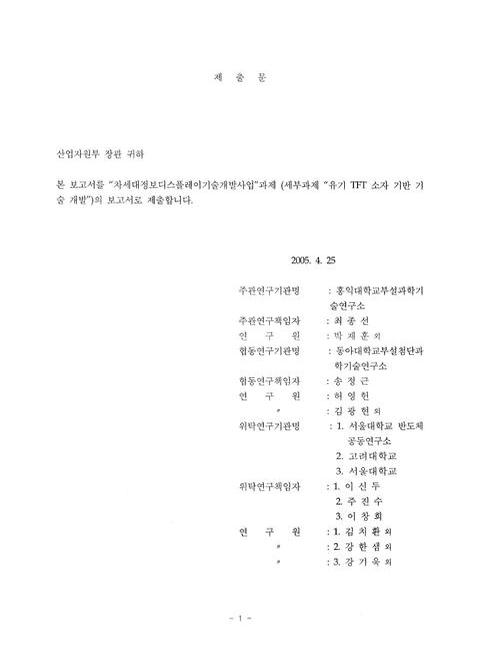
제출문=1,2,1
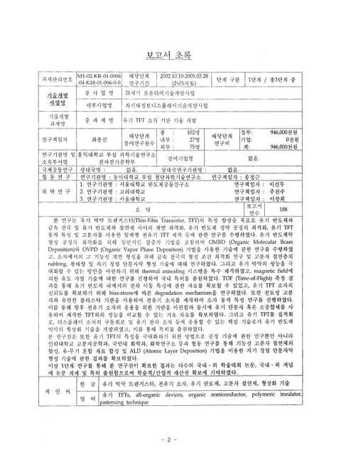
보고서 초록/최종선=2,3,1
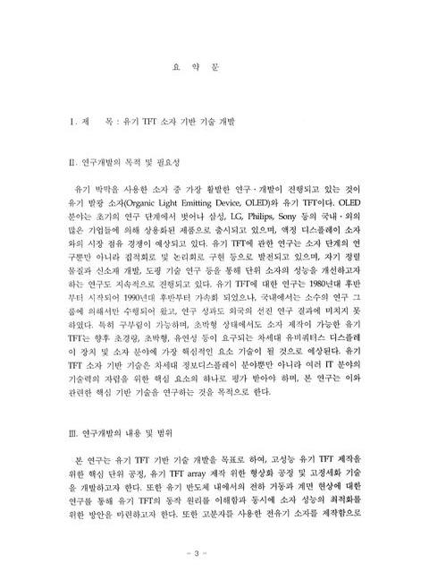
요약문=3,4,3
SUMMARY=6,7,1
CONTENTS=7,8,3
목차=10,11,3
제1장. 연구개발과제의 개요=13,14,3
제2장. 국내외 기술개발 현황=16,17,1
제1절. 전유기/플렉시블 디스플레이=16,17,1
제2절. 유기 박막트랜지스터=17,18,5
제3장. 연구개발 수행 내용 및 결과=22,23,1
제1절. 유기 박막 형성 공정 및 열처리 기술 연구=22,23,1
1. 유기 박막 형성 공정 최적화 및 기술 개발=22,23,1
(1) 성막 속도 제어를 이용한 유기 반도체 막과 소자 특성 연구=22,23,3
(2) OMBD 방식을 이용한 유기 박막 성막 공정 연구=24,25,8
(3) OVPD 방식을 이용한 유기 박막 성막 공정 연구=32,33,2
2. 유기 박막의 열처리 기술 개발 및 특성 연구=34,35,4
제2절. 고효율 절연층 형성 기술 및 소재 개발 연구=38,39,1
1. 절연층 구조 및 소재에 대한 연구=38,39,1
(1) 적층 구조의 절연층 특성 연구=38,39,1
(2) PVAc 특성 연구=39,40,2
(3) Cross-linked PVP 특성 연구=41,42,5
2. 새로운 절연소재 개발 연구=45,46,1
(1) 광반응기를 치환한 PVP의 합성 및 특성 연구=45,46,3
(2) 자기정렬기를 치환한 PVP의 합성 및 특성 연구=47,48,3
(3) PVAc-Clay 혼합 절연체 개발 및 특성 연구=49,50,4
(4) PVP-TiO₂혼한 절연체 개발 및 특성 연구=52,53,2
(5) 새로운 절연체 개발=53,54,2
3. 절연층의 기타 특성 연구=54,55,1
(1) PVP 막의 어닐링에 따른 특성 연구=54,55,2
(2) PVP 막의 condensation 효과=55,56,1
(3) PVP와 PMMA 절연 특성에 따른 소자 성능 비교=56,57,1
제3절. 소자 내의 단위 계면에 대한 특성 연구=57,58,1
1. 금속-유기 반도체 계면 연구=57,58,1
(1) Au 성막 속도 제어데 따른 유기 TFT 특성 연구=57,58,3
(2) 유기 반도체-전극 계면 특성을 통한 유기 반도체 물질의 배향 질서도 향상=59,60,4
(3) O₂plasma를 이용한 게이트 전극의 표면 처리 특성 연구=62,63,5
(4) MNB 전극 도포 효과=66,67,3
2. 절연체-유기 반도체 계면 연구=68,69,1
(1) Plasma를 이용한 PVP 표면 처리 특성 연구=68,69,3
(2) UV 소자에 의한 PVP 표면 처리=70,71,2
(3) ALD 법을 이용하여 SAMs 처리한 PVP 특성 연구=71,72,3
(4) 유기 반도체-절연체 계면 특성 향상을 통한 유기 반도체 물질의 배향 질서도 향상=73,74,3
(5) OTS의 channel 도표 효과=75,76,2
3. 계면 연구 결과의 집적=76,77,1
(1) 단위계면 특성 향상을 통한 유기 반도체 물질의 배향 질서도 향상 연구=76,77,2
(2) OTS/MNB 처리 특성 연구=78,79,2
제4절. 유기 (고)분자를 사용한 전유기 소자의 제작=80,81,5
제5절. 유기 박막 형상화 기술 개발=85,86,8
제6절. 유기 TFT 특성 및 기타 관련 연구=93,94,1
1. PVP를 절연층으로 사용한 유기 TFT의 Bias stress 특성 연구=93,94,2
2. 유기 반도체 분자 배향 제어 특성 연구=95,96,2
3. 전극의 위치와 두께에 따른 소자 특성 연구=96,97,4
4. 관련 장비의 설계ㆍ제작=99,100,1
(1) 유기물 정제 시스템 구축=99,100,1
(2) 열처리용 특수 오븐의 설계ㆍ제작=100,101,1
(3) 4"급 대면적 유기 박막 성막용 OVPD 시스템 설계 및 제작=100,101,5
5. 유기 TFT 및 TOF-PC 실험의 비교분석을 통한 전하수송 특성 연구=104,105,3
6. 전극/유기 반도체에서의 접촉 저항 감소를 통한 유기 TFT 성능 향상 연구=106,107,5
7. 용액 공정이 가능한 n-type Flexible 유기 TFT 제작=110,111,2
제7절. 유기 TFT 응용 소자=112,113,1
1. Pentacene TFT를 이용한 IC 회로=112,113,2
2. 유기 TFT-OLED 단위 픽셀 설계 및 제작=113,114,4
3. AM-OLED 디스플레이 패널 설계=116,117,1
(1) AM-OLED의 설계=116,117,3
(2) AM-OLED의 설계 조건=118,119,4
(3) AM-OLED 구동 회로 설계=121,122,3
(4) AM-OLED 디스플레이 패널 제작=123,124,4
제4장. 목표달성도 및 관련분야에의 기여도=127,128,1
제1절. 연구개발목표 및 평가의 착안점=127,128,6
제2절. 연구개발목표의 달성도=133,134,15
제3절. 관련분야에의 기여도=148,149,2
제5장. 연구개발결과의 활용계획=150,151,1
제1절. 연구개발결과의 활용=150,151,2
제2절. 추가연구의 필요성=152,153,2
제6장. 연구개발과정에서 수집한 해외과학기술정보=154,155,3
제7장. 참고문헌=157,158,2
Appendix=159,160,30
영문목차
[title page etc.]=0,1,7
CONTENTS=7,8,6
Chapter 1. Over View of the Research=13,14,3
Chapter 2. Domestic/International Status of the Technology Development=16,17,1
Paragraph 1. All-Organic Display/Flexible Display=16,17,1
Paragraph 2. Organic Thin Film Transistors=17,18,5
Chapter 3. Research Results=22,23,1
Paragraph 1. Organic Film Deposition Process & Thermal Treatment Techniqe=22,23,1
1. Process Optimization & Technique Development=22,23,1
(1) Deposition Rate Optimization=22,23,3
(2) OMBD Process=24,25,8
(3) OVPD Process=32,33,2
2. Thermal Treatment Technique=34,35,4
Paragraph 2. High-Performance Insulator Deposition & Material Development=38,39,1
1. Insulator Structure & Material Development=38,39,1
(1) Stacked Insulator Structure=38,39,1
(2) Characteristics of PVAc as a Gate Insulator=39,40,2
(3) Characteristics of Cross-1inked PVP as a Gate Insulator=41,42,5
2. Development of New Dielectric Materials=45,46,1
(1) New PVP with Photo-Reactive Group=45,46,3
(2) New PVP with Self-Assembled Group=47,48,3
(3) PVAc-Clay Composite=49,50,4
(4) PVP -TiO₂ Composite=52,53,2
(5) New Gate Insulator=53,54,2
3. Additional Investigation on the Gate Insulator=54,55,1
(1) Annealing Effect of PVP=54,55,2
(2) Condensation Effect of PVP=55,56,1
(3) Comparison of the performance according to the insulating properties (PVP vs. PMMA)=56,57,1
Paragraph 3. Investigation on the Unit Interface in OTFTs=57,58,1
1. Interface between Metal and Organic Layer=57,58,1
(1) Effect of the Deposition Rate of Au on the Device Performance=57,58,3
(2) Rubbing and Surfactant Effect=59,60,4
(3) O₂Plasma Treatment=62,63,5
(4) MNB Treatment=66,67,3
2. Interface between Insulator and Organic Layer=68,69,1
(1) Plasma Treatment on the surface of PVP=68,69,3
(2) UV Treatment on the surface of PVP=70,71,2
(3) SAMs Formation using ALD on the surface of PVP=71,72,3
(4) Effects of Interface Modification on the Molecular Ordering=73,74,3
(5) OTS Treatment=75,76,2
3. Integration of the Interface Modification=76,77,1
(1) Effects of Interface Modifications on the Molecular Ordering=76,77,2
(2) OTS/MNB Treatment=78,79,2
Paragraph 4. Fabrication & Characterization of All Organic Transistors=80,81,5
Paragraph 5. Patterning Technique for High Resolution Organic Film=85,86,8
Paragraph 6. Characteristics of Organic TFTs & Additional Research=93,94,1
1. Bias Stress in the Device with PVP as a Gate Insulator=93,94,2
2. Study on the Molecular Ordering using Rubbing Technique=95,96,2
3. Effects of Electrode Position & Thickness on the Device Performance=96,97,4
4. Equipment Developments=99,100,1
(1) Purification System=99,100,1
(2) Thermal Treatment System=100,101,1
(3) OVPD System for 4" Wafer=100,101,5
5. TOF-PC Results=104,105,3
6. Effects of Contact Resistance on the Device Performance=106,107,5
7. Soluble n-type Flexible Device=110,111,2
Paragraph 7. Applications=112,113,1
1. IC Fabrication Using Pentacene based TFTs=112,113,2
2. OTFT-OLED Unit Pixcel Design=113,114,4
3. AM-OLED Panel Fabrication=116,117,1
(1) AM-OLED Design=116,117,3
(2) Conditions of AM-OLED Design=118,119,4
(3) Driving Circuit for AM-OLED=121,122,3
(4) AM-OLED Panel=123,124,4
Chapter 4. Degree for Achieving the Research Goal & Contribution to Related Fields=127,128,1
Paragraph 1. The Research Goals & Point Aimed=127,128,6
Paragraph 2. Degree for Achieving the Research Goals=133,134,15
Paragraph 3. Contribution to Related Fields=148,149,2
Chapter 5. Plans of Applying the Research Results=150,151,1
Paragraph 1. Plans of Applying the Research Results=150,151,2
Paragraph 2. Necessities of Further Works=152,153,2
Chapter 6. Information obtained while carrying out the research=154,155,3
Chapter 7. References=157,158,2
Appendix=159,160,30
*표시는 필수 입력사항입니다.
| 전화번호 |
|---|
| 기사명 | 저자명 | 페이지 | 원문 | 기사목차 |
|---|
| 번호 | 발행일자 | 권호명 | 제본정보 | 자료실 | 원문 | 신청 페이지 |
|---|
도서위치안내: / 서가번호:

우편복사 목록담기를 완료하였습니다.
*표시는 필수 입력사항입니다.
저장 되었습니다.
