
 대표어
대표어




권호기사보기
| 기사명 | 저자명 | 페이지 | 원문 | 기사목차 |
|---|
결과 내 검색
동의어 포함
목차
표제지=0,1,1
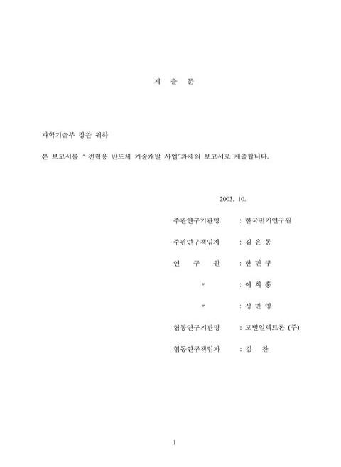
제출문=1,2,2
요약문=3,4,6
SUMMARY=9,10,5
CONTENTS=14,15,3
목차=17,18,5
제1장 연구개발과제의 개요=22,23,1
제1절 전력용 반도체 연구의 필요성=22,23,1
제2절 연구개발의 목표 및 내용=23,24,1
1. 과제별 연구개발 최종 목표=23,24,1
2. 연도별 연구개발 목표=24,25,3
제3절 추진전략 및 방법=27,28,2
제4절 연구개발 추진체계=28,29,2
제5절 기대효과=29,30,1
제6절 활용방안=30,31,2
제2장 4,500V급 SOC용 IGCT소자 개발=32,33,1
제1절 개요=32,33,1
1. 연구개발의 목적=32,33,1
가. 연구개발의 최종목표=32,33,1
나. 연구개발의 범위=33,34,1
다. 연구개발 추진체계=34,35,1
2. 연구개발의 필요성 및 중요성=35,36,1
가. 연구개발의 필요성=35,36,1
나. 연구개발의 중요성=36,37,2
제2절 국내외 기술개발 현황=37,38,1
1. 해외연구동향=37,38,3
2. 국내연구동향=39,40,2
제3절 연구개발수행 내용 및 결과=40,41,1
1. 서론=40,41,3
2. IGCT 소자 설계=42,43,1
가. 해석적인 방법을 통한 설계=42,43,12
나. 4500V급 IGCT 시제품 제작을 위한 일괄공정 설계=53,54,5
3. 소자제작을 위한 단위공정 실험=57,58,13
4. 패턴 마스크 설계 및 제작=69,70,5
5. 패키지 설계 및 제작=73,74,5
6. 게이트 구동 Unit 분석 및 제작=77,78,1
가. IGCT 소자 구동 드라이버의 개요=78,79,1
나. GCT 소자 구동 드라이버의 블록별 회로=78,79,8
다. 시작품 제작=85,86,1
라. 결과=86,87,1
7. 완성소자 특성평가=86,87,4
8. 결론=89,90,3
제4절 목표달성도 및 관련분야에의 기여도=91,92,3
제5절 연구개발결과의 활용계획=94,95,1
1. 타 연구에의 응용 및 기업화 추진방안=94,95,3
2. 추가연구의 필요성=96,97,2
제6절 연구개발과정에서 수집한 해외과학기술정보=97,98,3
제7절 참고문헌=99,100,2
제3장 1200V급 고신뢰성 MOS 구동 사이리스터 개발=101,102,1
제1절 서론=101,102,1
1. 연구의 목적 및 필요성=101,102,4
2. 연구 개발의 내용 및 범위=104,105,1
가. 연구개발의 최종목표=104,105,2
나. 연차별 연구개발 목표 및 내용=106,107,1
제2절 국내외 기술개발 현황=107,108,3
제3절 연구개발수행 내용 및 결과=109,110,1
1. 연구 개발의 접근방법=109,110,1
가. 연구의 접근 방법=109,110,2
나. 연구 진행도=111,112,1
2. 연구 내용 및 결과 요약=112,113,1
가. MOS 구동 사이리스터 자료 수집 및 분석=112,113,1
나. 소자 설계 및 시뮬레이션=112,113,1
다. 상세 도면 설계 Mask 용Layout=112,113,2
라. 단위공정 확립=113,114,1
마. 공정 설계 및 체계 완료 (run sheet 작성)=113,114,1
바. MOS 구동 사이리스터 단위-셀 소자의 제작=113,114,2
사. MOS 구동 사이리스터 단위-셀 소자의 측정=114,115,1
아. 1200V급 MOS 구동형 다이리스터의 Multi-cell 및 시작품 설계 및 제작=114,115,1
자. 제작한 시제품의 특성 측정 및 신뢰성 평가=114,115,2
차. 보호회로 설계=115,116,1
카. 응용 연구=115,116,2
3. 상세 연구 결과=116,117,1
가. 트렌치 게이트와 자기정렬 corrugated P-베이스를 이용한 새로운 베이스 저항제어 사이리스터=116,117,7
나. 고내압 특성을 위한 진성영역과 트렌치 구조를 MOS 구동 사이리스터=122,123,8
다. 1200V 항복 전압 설계 연구=129,130,2
라. 단위 소자 특성 측정을 위한 소자 패키지와 turn-off 측정=130,131,2
마. 단위 소자의 Layout 설계=131,132,3
바. Trench gate CB-BRT의 최대 제어 가능 전류 향상을 위한 설계 변수의 영향분석=133,134,6
사. 전류포화특성과 턴-오프 특성이 개선된 새로운 전도도 변조 사이리스터=138,139,7
아. 실리콘 식각과 산화막을 이용한 항복전압 개선=144,145,5
자. 3-D 시뮬레이션을 통한 MOS 구동 사이리스터의 특성 향상 효과 분석=148,149,7
차. 고전압 전류 포화를 위한 새로운 EST (Emitter Switched Thyristor)보호회로=154,155,5
카. 컬렉터-이미터 전압 (Vce)감지를 통한 전력용 소자의 단락 회로 유지 기능 향상을 위한 새로운 보호회로=158,159,7
타. 1200V급 고 신뢰성 MOS 구도 사이리스터 설계 및 제작=164,165,9
4. 연구성과=172,173,5
제4절 연구개발목표 달성도 및 대외기여도=177,178,1
1. 연도별 연구목표 및 내용=177,178,1
2. 연도별 연구개발목표 달성도=178,179,8
제5절 연구개발결과의 활용계획=185,186,1
1. 타연구에의 응용 및 기업화 추진방안=185,186,2
제6절 참고문헌=186,187,2
제4장 통신전원용 220VAC 입력 SMPS IPM 개발=188,189,1
제1절 연구개발의 배경=188,189,1
제2절 연구개발의 내용 및 범위=188,189,1
1. 최종연구 목표=189,190,2
제3절 연구개발 결과=191,192,1
1. 1.5kW급 Phase-Shifted ZVS FB-SMPS 개발=191,192,1
가. IPM적용 검토=191,192,1
나. 1.5kW급 Phase shifted ZVS FB-SMPS 설계=191,192,4
2. 통신전원용 IPM 개발=194,195,1
가. IPM의 열설계=194,195,2
나. 열해석 결과=196,197,2
다. IPM 구조 설계=197,198,2
3. IPM 제조공정기술=198,199,3
가. 칩 엘리멘트(chip element) 제조공정=201,202,1
나. 베이스 제조공정=202,203,1
다. 베이스솔더링 평가=203,204,4
라. 와이어본딩(WIRE BONDING) 공정=206,207,3
마. 몰딩공정=208,209,1
바. 검사공정=208,209,4
4. 1.5kW급 Phase shifted ZVS FB-SMPS=211,212,6
제4절 결론 및 향후 활용 계획=217,218,2
제5절 참고문헌=219,220,1
제5장 BkV급 초고전압 다이오드 개발=220,221,1
제1절 연구의 필요성=220,221,1
1. 연구의 목적 및 필요성=220,221,2
2. 연구 개발의 내용 및 범위=221,222,1
가. 연구개발의 목표=222,223,1
나. 연구 범위 및 연구수행 방법=222,223,2
제2절 국내외 기술개발 현황=223,224,2
제3절 연구개발수행 내용 및 결과=225,226,1
1. 8kV급 전자렌지용 고압다이오드 개발=225,226,1
가. 개발목표 선정=225,226,2
나. 제품설계=226,227,7
다. 제조 공정 확립=233,234,2
라. 전기적 특성=234,235,5
마. 결과 요약=238,239,3
2. TVS 다이오드 개발=240,241,1
가. 고전압 Surge 보호 Diode(TVS Diode) 개요=240,241,2
나. 소자설계=242,243,3
다. 공정설계 및 개발=245,246,2
라. 전기적특성 평가=247,248,5
제6장 전력용 반도체 사업단 보고서=252,253,1
제1절 개요=252,253,1
1. 전력용 반도체의 정의 및 개발 필요성=252,253,2
2. 목적 및 기대효과=253,254,3
제2절 연구개발수행 내용 및 결과=255,256,1
1. 진도관리=255,256,1
2. homepage 구축 및 사업단 홍보=255,256,6
3. 정보 교류 및 전문가 초청=260,261,1
4. 연구성과 발표 실적=260,261,10
영문목차
[title page etc.]=0,1,14
CONTENTS=14,15,8
Chap. 1. Outline of the research project=22,23,1
Section 1. Necessities of Power Semiconductor research=22,23,1
Section 2. Goal & contents of the research=23,24,1
1. Final goals of each project=23,24,1
2. Annual research goal=24,25,3
Section 3. Method and strategy of research=27,28,2
Section 4. System of research organization=28,29,2
Section 5. Expected effects=29,30,1
Section 6. Applications of Results=30,31,2
Chap. 2. Development of 4500V Integrated Gate-Commutated Thyristor devices for Social Object Capital=32,33,1
Section 1. Outline=32,33,1
1. Goal of research=32,33,3
2. Necessity and importance of research=35,36,3
Section 2. State of the art=37,38,1
1. Abroad=37,38,3
2. Domestic=39,40,2
Section 3. Research subject and results=40,41,1
1. Introduction=40,41,3
2. Design of IGCT device=42,43,16
3. Unit process experiment for the fabrication of device=57,58,13
4. Design and fabrication of pattern mask=69,70,5
5. Design and fabrication of package=73,74,5
6. analysis and fabrication of gate driver unit=77,78,10
7. Characterization of fabricated device=86,87,4
8. Conclusion=89,90,3
Section 4. Achievement and Contribution=91,92,3
Section 5. Application of results=94,95,1
1. Method for application to other research and commercialization=94,95,3
2. Necessity of additional research=96,97,2
Section 6. Technical information obtained during research=97,98,3
Section 7. References=99,100,2
Chap. 3. Development of high reliability 1200V MOS-Cated thyristor=101,102,1
Section 1. Introduction=101,102,1
1. Goal and necessity=101,102,4
2. Contents and area of research=104,105,3
Section 2. State of the art=107,108,3
Section 3. Subjects and results=109,110,1
1. Approaching methods=109,110,3
2. Results and summary=112,113,5
3. Results in detail=116,117,57
4. Research product=172,173,5
Section 4. Achievement and Contribution=177,178,1
1. Annual Goals and contents=177,178,1
2. Annual degree of achievement=178,179,8
Section 5. Plan for result application=185,186,1
1. Method for application to other research and commerciallization=185,186,2
Section 6. References=186,187,2
Chap. 4. The Development of 220VAC Input SMPS Intelligent Power Module(IPM) far Telecommunication Application=188,189,1
Section 1. Background=188,189,1
Section 2. Subjects and results=188,189,1
1. Final goal of research=189,190,2
Section 3. Results=191,192,1
1. Development of 1.5kW class Phase-Shifted ZVS FB-SMPS=191,192,1
2. Development of IPM for telecommunication power supply=191,192,8
3. Fabrication technology of IPM=198,199,14
4. 1.5kW class Phase shifted ZVS FB-SMPS=211,212,6
Section 4. Conclusion and future work217=217,218,2
Section 5. References=219,220,1
Chap. 5. Development of 8kV class high voltage diode=220,221,1
Section 1. Necessity of research=220,221,1
1. Necessity and Goal of research=220,221,2
2. Subjects and Contents=221,222,3
Section 2. State of the art=223,224,2
Section 3. Subjects and results=225,226,1
1. Development of 8kV class high voltage diode for microwave range=225,226,16
2. Development of TVS diode=240,241,12
Chap. 6. Report of Power Semiconductor Research Organization=252,253,1
Section 1. Outline=252,253,1
1. Definition and develoment necessity of power semiconductor=252,253,2
2. Aims and expected effect=253,254,3
Section 2. Subject and results=255,256,1
1. Manage of progress=255,256,1
2. Establishment of homepage and organization advertize=255,256,6
3. Communication of information and invitation of specialist=260,261,1
4. Publication List=260,261,10
*표시는 필수 입력사항입니다.
| 전화번호 |
|---|
| 기사명 | 저자명 | 페이지 | 원문 | 기사목차 |
|---|
| 번호 | 발행일자 | 권호명 | 제본정보 | 자료실 | 원문 | 신청 페이지 |
|---|
도서위치안내: / 서가번호:

우편복사 목록담기를 완료하였습니다.
*표시는 필수 입력사항입니다.
저장 되었습니다.
