
 대표어
대표어
권호기사보기
| 기사명 | 저자명 | 페이지 | 원문 | 기사목차 |
|---|
결과 내 검색
동의어 포함
목차
표제지=0,1,1
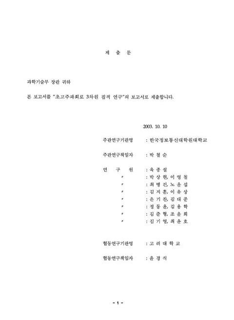
제출문=1,2,1
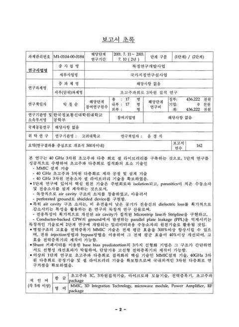
보고서 초록/박철순=2,3,1
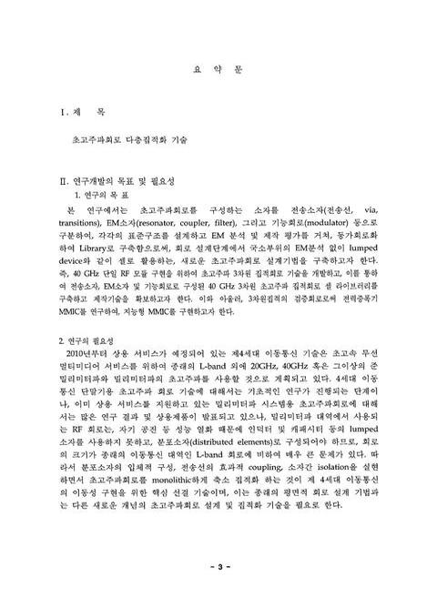
요약문=3,4,8
SUMMARY=11,12,8
CONTENTS=19,20,4
목차=23,24,4
제1장 연구개발과제의 개요=27,28,1
제1절 연구개발의 목적=27,28,1
제2절 연구개발의 필요성=27,28,1
1. 기술적 측면=27,28,3
2. 경제.산업적 측면=29,30,2
3. 사회.문화적 측면=30,31,2
제3절 연구개발 목표 및 내용=31,32,1
1. 연구개발의 최종목표=31,32,1
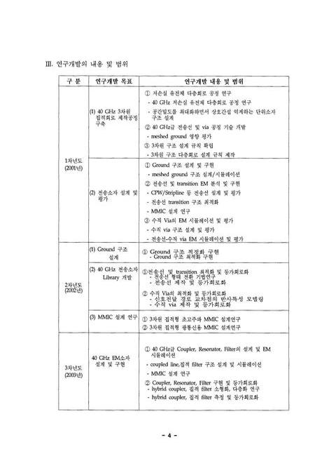
2. 단계별/연차별 연구개발 목표 및 내용=32,33,1
가. 단계별 연구목표=32,33,1
나. 1단계 연차별 연구개발 목표=33,34,1
다. 2단계 연차별 연구개발 목표=34,35,1
제2장 국내외 기술개발 현황=35,36,1
제1절 국내의 기술동향 및 수준=35,36,2
제2절 국외의 기술동향 및 수준=36,37,2
제3장 연구개발 수행 내용 및 결과=38,39,1
제1절 3차원 다층회로 연구=38,39,1
1. 40㎓ 저손실 다층회로 공정연구=38,39,1
가. 초고주파 3차원 다층회로 구현을 위한 공정=38,39,1
(1) 선폭(line width)/선간거리(spacing) 측정=39,40,1
(2) Conductor의 면 저항(sheet resistance) 및 via 저항 측정=40,41,1
(3) 유전상수(dielectric constant) 측정=40,41,1
(4) 층별 정렬(vertical alignment) 정도 분석=41,42,1
(5) 유전체 기판과 conductor 수축(shrinkage) 특성 분석=41,42,1
나. 다층회로 설계 규칙 (design rule)=42,43,2
2. Air cavity를 이용한 저 손실 전송선 연구=43,44,1
가. Embedded air cavity 공정=43,44,1
나. Air cavity를 이용한 저 손실 microstrip line 구현=44,45,5
다. Air cavity를 이용한 저 손실 stripline 구현=48,49,5
3. 3차원 다층회로 셀 라이브러리 연구=52,53,1
가. 전송선 라이브러리=52,53,1
(1) 전송선 제작=52,53,1
(가) Microstrip line=52,53,1
(나) Grounded coplanar waveguide (CPWG)=53,54,1
(다) Stripline=53,54,2
(2) 전송선 Loss 특성 및 effective dielectric constant 분석=54,55,1
(가) λg/4 T-resonator 제작 및 측정=54,55,2
(나) 전송선의 특성=56,57,2
나. Vertical Via transition 라이브러리=58,59,1
(1) Vertical transition 연구의 필요성=58,59,1
(2) Vertical transition 구조 설계=58,59,1
(가) Microstrip line to embedded microstrip line transition=59,60,1
(나) CPW to embedded CPW transition=59,60,1
(다) CPW to stripline transition=59,60,1
(라) Microstrip line to embedded CPW=59,60,3
(3) Vertical transition 제작 및 측정=61,62,1
(가) Microstrip line to embedded microstrip line transition=61,62,2
(나) CPW to embedded CPW transition=62,63,2
(다) CPW to stripline transition=63,64,2
(라) Microstrip line to embedded CPW=64,65,1
(4) Vertical transition 모델링=65,66,1
(가) CPW to stripline transition 모델링=65,66,2
(나) CPW to embedded CPW 모델링=66,67,2
4. Ground 구조 연구=67,68,1
가. Meshed ground의 isolation 특성분석=67,68,3
나. Ground 구조에 따른 전송선 특성 분석=69,70,1
다. Ground 구조에 따른 capacitor와 inductor의 특성분석=70,71,1
5. Air cavity를 이용한 CPW구조에서 PPL 억제 연구=70,71,1
가. CPW 구조에서 Leakage mechanism=70,71,4
6. 기타 연구 성과=73,74,1
가. Kaband band pass filter 구현=73,74,1
(1) Ka-대역 Band pass filter 연구의 필요성=73,74,2
(2) Ka-대역 Band pass filter 설계=74,75,3
(3) Ka-대역 Band pass filter 제작 및 측정=76,77,2
(4) 요약=77,78,1
나. 3차원 집적 30㎓ 전력증폭기 모듈 구현=77,78,2
(1) RF 입 출력 단자 설계=78,79,1
(2) 모듈 제작=78,79,2
(3) 모듈 측정 결과=79,80,1
제2절 초고주파 전력증폭기 MMIC 설계 연구=80,81,1
1. 고선형 전력증폭기 기술=80,81,1
가. 병렬 커패시터 선형화기=80,81,2
나. 커패시터 결합 선형화기=81,82,2
다. 역 다이오드 결합 선형화기=82,83,3
2. 고효율 전력증폭기 기술=84,85,1
가. 전류 바이패스 기술=84,85,4
나. 전류 주입 기술=87,88,4
다. Dual-Chain 전력증폭기 기술=90,91,4
라. 지능형 능동 전력증폭기 기술=93,94,3
3. 다중대역/다중모드 전력증폭기 기술=95,96,5
4. 온도 및 전압 변화에 대한 안정화 기술=99,100,5
5. 5㎓ 대역 WLAN용 전력증폭기=104,105,3
제3절 광통신용 초고속 데이터 통신 수신단 회로 설계=106,107,1
1. 이론적,실험적 접근방법=106,107,1
2. 연구결과=107,108,1
가. 공통 에미터 전치증폭기=107,108,5
나. 인덕티브 버퍼단을 이용한 InGaP/GaAs HBT 전치증폭기 회로 설계=112,113,4
다. 차등증폭기구조의 InGaP/GaAs HBT 전치증폭기 회로 설계=115,116,4
라. 광통신용 초고속 제한증폭기회로 설계=118,119,3
제4절 MMIC Behavioral Modeling 연구 (위탁과제)=121,122,1
1. 점근선 기법=122,123,1
2. 인공신경망 기법=122,123,1
3. Behavioral model 생성=123,124,1
4. Behavioral model을 이용한 MMIC 전력증폭기 비선형 특성 시뮬레이션=123,124,3
5. 연구결과=125,126,5
제4장 목표 달성도 및 관련분야 기여도=130,131,1
제1절 목표 달성도=130,131,1
1. 총괄 연구목표 달성도=131,132,1
2. 3차원 다층회로 연구=132,133,2
3. MMIC 연구=134,135,1
4. 추가 연구결과=135,136,1
제2절 관련분야 기여도=135,136,1
1. 3차원 다층회로 연구=135,136,1
가. 기술적인 기여=135,136,1
나. 산업적 기여=136,137,1
2. MMIC 연구=136,137,1
가. 기술적인 기여=136,137,1
나. 산업적 기여=136,137,1
3. 초고속 광통신용 MMIC 연구=136,137,1
가. 기술적인 기여=136,137,1
제5장 연구개발 결과의 활용계획=137,138,1
제1절 3차원 다층회로 연구결과 활용계획=137,138,1
1. 저 손실 초고주파 3차원 다층회로 제작 및 셀 라이브러리 기술=137,138,1
가. 기술적인 측면=137,138,1
나. 산업적인 측면=137,138,1
2. 초고주파 3차원 다층회로 셀 라이브러리 기술=137,138,1
가. 기술적인 측면=137,138,2
나. 산업적인 측면=138,139,1
3. Air cavity를 이용한 초고주파 3차원 다층회로 개발 기술=138,139,1
가. 기술적인 측면=138,139,1
나. 산업적인 측면=138,139,1
제2절 MMIC 연구결과 활용계획=138,139,1
1. 고효율 MMIC 전력증폭기=138,139,1
가. 기술적인 측면=138,139,1
나. 산업적인 측면=138,139,2
2. 고선형 MMIC 전력증폭기=139,140,1
가. 기술적인 측면=139,140,1
나. 산업적인 측면=139,140,1
3. 광 MMIC 기술=139,140,1
가. 기술적인 측면=139,140,1
나. 산업적인 측면=139,140,1
제6장 해외과학기술 정보=140,141,1
제1절 3차원 다층회로 연구분야=140,141,2
제2절 MMIC 연구 분야=142,143,1
제3절 광통신 MMIC 연구분야=143,144,1
제7장 참고문헌=144,145,18
영문목차
[title page etc.]=0,1,19
CONTENTS=19,20,8
Chapter 1. Outline of The Research Development Subject=27,28,1
Section 1. Object of Research Development=27,28,1
Section 2. Necessity of Research Development=27,28,1
1. Technical Aspect=27,28,3
2. Economic & Industrial Aspect=29,30,2
3. Social & Cultural Aspect=30,31,2
Section 3. Goal and Substance of Research Development=31,32,1
1. Final Goals and Activities=31,32,1
2. Goals and Activities=32,33,1
A. Research Plan for the Phase I and II=32,33,1
B. Annual Research Plan for The Phase I=33,34,1
C. Annual Research Plan for The Phase II=34,35,1
Chapter 2. Technical Trends=35,36,1
Section 1. Domestic Technical Trend=35,36,2
Section 2. International Technical Trend=36,37,2
Chapter 3. Achievement and Result of Research Development=38,39,1
Section 1. Research of 3D Multi-layer Circuit=38,39,1
1. Research of 40 GHz Low-loss Multi-layer Circuit Process=38,39,1
A. Process for Microwave 3D Multi-layer Circuit Embodiment=38,39,1
(1) Measurement of Line Width and Spacing=39,40,1
(2) Measurement of Couductor's Sheet Resitance and Via Resistance=40,41,1
(3) Measurement of Dielectric Constant=40,41,1
(4) Analysis of Vertical Alignment Rate=41,42,1
(5) Analysis of Dielectric Substrate and Conductor shrinkage=41,42,1
B. Multi-layer Circuit Design Rule=42,43,2
2. Research of Low-loss Transmission Line Using Air Cavity=43,44,1
A. Embedded Air Cavity Process=43,44,1
B. Embodiment of Low-loss Microstrip Line Using Air Cavity=44,45,5
C. Embodiment of Low-loss Stripline Using Air Cavity=48,49,5
3. Research of 3D Multi-layer Cell Library=52,53,1
A. Transmission Line Library=52,53,1
(1) Production of Transmission Line=52,53,1
(a) Microstrip Line=52,53,1
(b) Grounded Coplanar Waveguide (CPWG)=53,54,1
(c) Stripline=53,54,2
(2) Analysis of Transmission Line Loss/Effective Dielectric Constant=54,55,1
(a) Production and Measurement of Xg/4 T-resonator=54,55,2
(b) Characteristic of Transmission Line=56,57,2
B. Vertical Vial Transition Library=58,59,1
(1) Necessity of Vertical Transition Research=58,59,1
(2) Design of Vertical Transition Structure=58,59,1
(a) Microstrip Line To Embedded Microstrip line Trasition=59,60,1
(b) CPW To Embedded CPW Trasition=59,60,1
(c) CPW To Stripline Trasition=59,60,1
(d) Microstrip Line to Embedded CPW=59,60,3
(3) Production and Measurement of Vertical Transition=61,62,1
(a) Microstrip Line to Embedded Microstrip Line Transition=61,62,2
(b) CPW To Embedded CPW Trasition=62,63,2
(c) CPW To Stripline Transition=63,64,2
(d) Microstrip Line to Embedded CPW=64,65,1
(4) Vertical Transition Modeling=65,66,1
(a) CPW to Stripline Trasition Modeling=65,66,2
(b) CPW to Embedded CPW Modeling=66,67,2
4. Research of Ground Structure=67,68,1
A. Analysis of Meshed Ground isolation=67,68,3
B. Analysis of Transmission Line according to Ground Structure=69,70,1
C. Analysis of Capacitor/Inductor according to Ground Structure=70,71,1
5. Research of PPL Suppression in Air Cavity CPW=70,71,1
A. Leakage Mechanism in CPW Structure=70,71,4
6. The Other Research Results=73,74,1
A. Embodiment of Ka-band Band Pass Filter=73,74,1
(1) Necessity of Ka-band Band Pass Filter research=73,74,2
(2) Design of Ka-band Band Pass Filter=74,75,3
(3) Production and Measurement of Ka-band Band Pass Filter=76,77,2
(4) Summary=77,78,1
B. Embodiment of 3D Integrated 30 GHz Power Amplifier Module=77,78,2
(1) Design of RF Input and Output port=78,79,1
(2) Production of Module=78,79,2
(3) Mesurement of Module=79,80,1
Section 2. Research of Microwave Power Amplifier MMIC Design=80,81,1
1. Technology of High Linearity Power Amplifier=80,81,1
A. Chunt Capacitor Linearizer=80,81,2
B. Coupling Capacitor Linearizer=81,82,2
C. Coupling Reverse Diode Linearizer=82,83,3
2. Technology of High Efficient Power Amplifier=84,85,1
A. Technique of Bypassing Current=84,85,4
B. Technique of Current Injection=87,88,4
C. Dual-Chain Power Amplifier=90,91,4
D. Adaptive Power Amplifier=93,94,3
3. Technology of Multi-band Multi-mode power amplifier=95,96,5
4. Stabilization of Temperature/Voltage Variation=99,100,5
5. 5GHz WLAN Power Amplifier=104,105,3
Section 3. Research of High Speed Optical Receiver Circuit=106,107,1
1. Methods of Theoretical and Experimental Approach=106,107,1
2. Research Results=107,108,1
A. Common Emitter Transimpedance Amplifier=107,108,5
B. InGaP/GaAs HBT Transimpedance Amplifier Using Inductive Buffer=112,113,4
C. InGaP/GaAs HBT Differential Transimpedance Amplifier=115,116,4
D. High Speed Limiting Amplifier for Optical Communication=118,119,3
Section 4. Research of MMIC Behavioral Modeling=121,122,1
1. Asymptotic Line Technique=122,123,1
2. Artificial Nerve Technique=122,123,1
3. Formation of Behavioral Model=123,124,1
4. MMIC PA Non-linearity Simulation Using Behavioral Model=123,124,3
5. Research Results=125,126,5
Chapter 4. Rate of Goal Attainment & Contribution to Related Field=130,131,1
Section 1. Rate of Goal Attainment=130,131,1
1. Rate of Total Research Goal Attainment=131,132,1
2. 3D Multi-layer Research=132,133,2
3. MMIC Research=134,135,1
4. Additional Research Results=135,136,1
Section 2. Rate of Contribution to Related Field=135,136,1
1. 3D Multi-layer Research=135,136,1
A. Technical Contribution=135,136,1
B. Industrial Contribution=136,137,1
2. MMIC Research=136,137,1
A. Technical Contribution=136,137,1
B. Industrial Contribution=136,137,1
3. High Speed Optical MMIC Research=136,137,1
A. Technical Contribution=136,137,1
Chapter 5. Application Plan of Research Result=137,138,1
Section 1. Application Plan of 3D Multi-layer Circuit Research Result=137,138,1
1. Cell Library Technique of Low-loss Microwave 3D Multi-layer Circuit=137,138,1
A. Technical Aspect=137,138,1
B. Industrial Aspect=137,138,1
2. Cell Library Technique of Microwave 3D Multi-layer Circuit=137,138,1
A. Technical Aspect=137,138,2
B. Industrial Aspect=138,139,1
3. Technique of Microwave 3D Multi-layer Circuit Using Air Cavity=138,139,1
A. Technical Aspect=138,139,1
B. Industrial Aspect=138,139,1
Section 2. Application Plan of MMIC Research Result=138,139,1
1. High Efficient MMIC Power Amplifier=138,139,1
A. Technical Aspect=138,139,1
B. Industrial Aspect=138,139,2
2. High Linearity MMIC Power Amplifier=139,140,1
A. Technical Aspect=139,140,1
B. Industrial Aspect=139,140,1
3. Optical MMIC Technique=139,140,1
A. Technical Aspect=139,140,1
B. Industrial Aspect=139,140,1
Chapter 6. Information of International Science Technology=140,141,1
Section 1. Research Field of 3D Multi-layer Circuit=140,141,2
Section 2. Research Field of MMIC=142,143,1
Section 3. Research Field of MMIC for Optical Communication=143,144,1
Chapter 7. Reference=144,145,18
*표시는 필수 입력사항입니다.
| 전화번호 |
|---|
| 기사명 | 저자명 | 페이지 | 원문 | 기사목차 |
|---|
| 번호 | 발행일자 | 권호명 | 제본정보 | 자료실 | 원문 | 신청 페이지 |
|---|
도서위치안내: / 서가번호:

우편복사 목록담기를 완료하였습니다.
*표시는 필수 입력사항입니다.
저장 되었습니다.
