
 대표어
대표어
권호기사보기
| 기사명 | 저자명 | 페이지 | 원문 | 기사목차 |
|---|
결과 내 검색
동의어 포함
목차
[표제지]=0,1,1
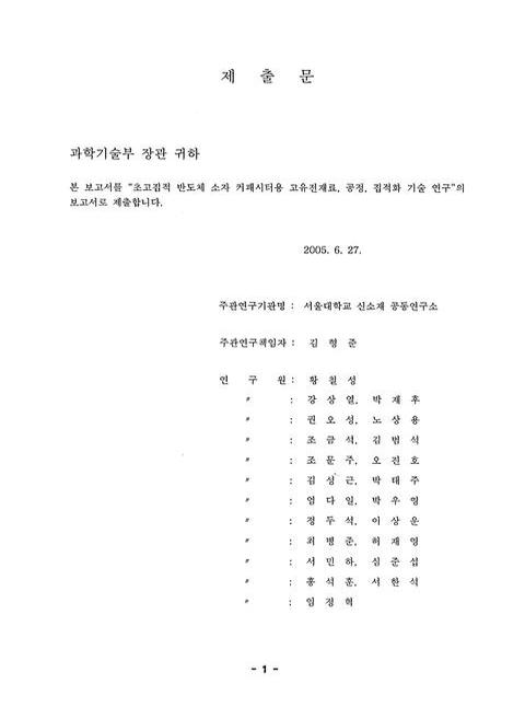
제출문=1,2,1
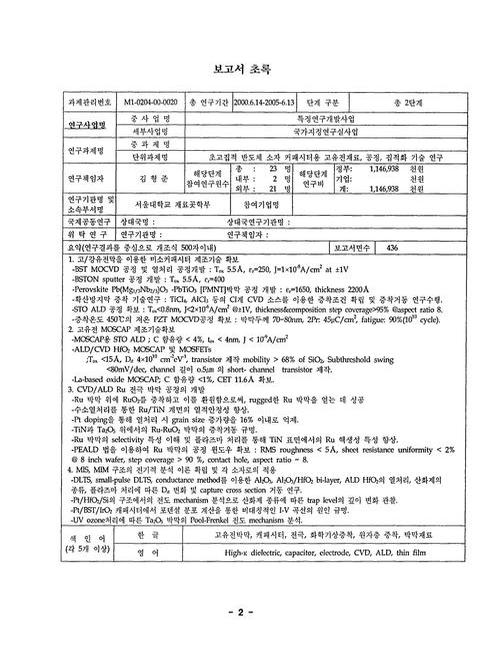
보고서 초록=2,3,1
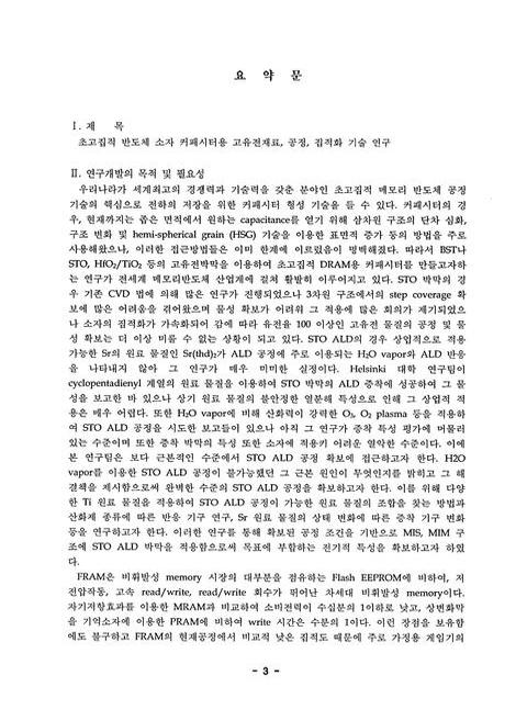
요약문=3,4,8
Summary=11,12,2
Contents=13,14,1
목차=14,15,1
제1장 연구개발 과제의 개요=15,16,2
제2장 국내외 기술개발 현황=17,18,2
제3장 연구개발수행 내용 및 결과=19,20,1
1단계 연구(2000.6.14-2002.6.13)=19,20,1
제1절 BST 박막의 증착 및 특성 분석=19,20,18
제2절 ALD 공정을 이용한 STO 고유전 박막 개발=37,38,10
제3절 Pb계 새로운 고유전 물질 탐색=47,48,8
제4절 MOCVD법에 의한 Ta₂O5 박막 형성 및 특성 평가(이미지 참조)=55,56,4
제5절 새로운 Gate Oxide용 고유전 물질 탐색연구=59,60,2
제6절 전기적, 화학적 구조적 분석 기술 구축=61,62,18
제7절 금속 전극 박막 증착 기술 연구=79,80,12
제8절 확산방지막 증착 기술 연구=91,92,5
2단계 연구(2002.6.14-2005.6.13)=96,97,1
제1절 고/강유전막을 이용한 미소커패시터 제조기술확보=96,97,89
제2절 Gate용 고유전 MOSCAP 제조기술확보=185,186,129
제3절 미소캐패시터용 Ru 전극 박막 공정의 개발=314,315,46
제4절 MIS, MIM 구조의 전기적 분석 이론 확립=360,361,21
제4장 목표 달성도 및 관련분야에의 기여도=381,382,5
제5장 연구개발결과의 활용계획=386,387,3
제6장 연구개발과정에서 수집한 해외과학기술정보=389,390,3
[제7장 참고문헌 등]=392,393,8
영문목차
[title page etc.]=0,1,11
Summary=11,12,2
[Contents etc.]=13,14,2
Chapter 1. Introduction=15,16,2
Chapter 2. State Of Art=17,18,2
Chapter 3. Research Of Detail=19,20,362
Chapter 4. Degree Of Reaching The Goal And Contribution=381,382,5
Chapter 5. Plan Of Utilizing The Research Results=386,387,3
Chapter 6. The Collected Scientific Information Of Overseas During Performing The Research Project=389,390,3
[Chapter 7. References, etc.]=392,393,8
jpg
Fig.9. TEM Image (a) And Composition (b) Of SrTiO₃Films Deposited With Single Source SrTi(DPM)₄(Tetraen)₂=33,34,1
Fig.10. Crossectional TEM Images Of BST Films On A) 150nm Diameter Hole And B) 230nm Diameter Hole, And c) Their Composition Variations. Precursor : Sr(THD)₂-Pmdt, Ti(THD)₂(O-iPr)₂=34,35,1
Fig.11. Cross Sectional TEM Image (a) And Compositions (b) Of SrTiO₃ Films Deposited On 150nm Diameter Hole. Presursor : Sr(METHD)₂, Ti(MPD)(THD)₂=35,36,1
Fig.12. Cross Sectional TEM Image Of SrTiO₃Films Deposited On 150nm Diameter Hole a) Without Dome Heating And b) With Dome Heating, And c) Their Compostion Variations On The Hole Wall. Presursor : Sr(METHD)₂, Ti(MPD)(THD)₂=36,37,1
Fig.25. SEM Image Of 0.9PMN-0.1PT Thin Film Using A Sol fabricated At (a) Elevated Temperature(110℃-124℃) With DEA, (b) Room Temperature With DEA, (c) Room Temperature With DEA+EG=53,54,1
Fig.28. SEM Image Of Ta₂O5 Thin Films Deposited Under Various Chamber Pressures(이미지참조)=57,58,1
Fig.31. HRTEM Image Of As-Deposited Si/Al₂O₃/HfO₂ Stack=65,66,1
Fig.32. HRTEM Image Of Si/ Al₂O₃/ HfO₂ Annelaed At 800℃=66,67,1
Fig.33. EDS Line Scanning Of Si/Al₂O₃/ HfO₂ Stack=67,68,1
Fig.36. A High-Resolution TEM Micrograph Of A Sample Annealed At 450℃ In H₂. The Thickness Of The Al₂O₃ Layer Is 5.8nm=73,74,1
Fig.45. Step Coverage Of Ru Thin Film=84,85,1
Fig.48. The Surface Morphologies Of (a)RuO₂/Ru Thin Film, (b) H₂-Annealed RuO₂/Ru Thin Film, (c) The Oxidized Film Of (b), And (d) H₂ Annealed Of (c)=88,89,1
Fig.49. The AFM Image Of Ru Thin Films (The Thickness Of (a) And (b) Are 200Å And 500Å, Respectively). (c) And (d) Are The AFM Images Of The Annealed Sample Of (a) And (b), Respectively=90,91,1
Figure3. a) AES, b) SEM, c) Cross-Sectional TEM Of SrO With H₂O Vapor=101,102,1
Figure9. Step Coverage Of a)TiO₂ And b)SrO On Trench Structure=107,108,1
Figure10. Crystallization Of As-Dep a)TiO₂ And b)SrO Films=108,109,1
Figure15. Cross-Sectional TEM Image Of STO Films On a) Si And b) Ru Substrate=122,123,1
Figure16. AFM Image And RMS Roughness Of STO AS A Function Of Number Of Cycle=123,124,1
Figure19. a)Cross-Sectional TEM Image Of STO Films On SiO₂ Contact Hole And b) Sr/Ti Atomic Ratio At The Various Points Shown In a) As A Function Of Deposition Temperature=126,127,1
Figure25. a) Bright-Field TEM, b) Z-Contrast Dark-Field Image Using A High-Angle Annular Dark Field Detector And c) Sr/Ti Atomic Ratio Of STO Film At The Various Poings Shown In A=132,133,1
Figure39. SEM Image Of As Dep. And Crystallized STO w/ And w/o Seed Layer=153,154,1
Figure46. (a) And (b) Cross-Section TEM Micrographs Of The Films Grown At 500℃ With The Type 3 Solution And The Oxygen Flow Rate Of 400 Sccm Through The Injector, And 200 Sccm Through Injector And 300 Sccm Through Shower-Ring Respectively=163,164,1
Figure56. SEM Surface Morphologies Of The Films Grown At Td's Of (a) 450, (b) 475, (c) 500 And (d) 525℃ On The SiO₂ Film Deposited By Plasma-Enhanced CVD With The Root-Mean-Squared Roughness Measured By AFM=176,177,1
Figure58. (a) SEM Micrograph Of A Film Grown At A Td Of 525oC On A Pt Substrate, And The SEM Micrographs Of Films Grown On Ir Substrates At (b) 475, (c) 500 And (d) 525℃=180,181,1
Figure60. SEM Micrograph Of A Lead Oxide Film Grown At A Td Of 525℃ With Oxygen Flow Rate Of 200 SCCM And A Tdof 5 Min And (b) Variation In The Layer Density Of A Lead Oxide Film As A Function Of The Oxygen Flow Rate A Td Of 525℃=182,183,1
Figure71. HRTEM Images Of HfO₂ Films Deposited With Hf[N(CH₃)₂]₄ And (a) H₂O, (b) O₃ In As-Deposited=198,199,1
Figure78. HRTEM Images Of (a) HfO₂/ Si, (b) In-Situ NH₃ Introduced HfO₂/ Si, (c) Ex-Situ NH₃ Annealed HfO₂/ Si Films=207,208,1
Figure82. HRTEM Images Of Poly-Si/HfO₂ Gate Dielectric/Si Channel Structures In Transistor;(a) H₂O-HfO₂,(b) O₃-HfO₂, And (c) O₃-HfO₂/O₃-SiO₂=213,214,1
Figure98. The HRTEM Images Of HfO₂ Films Grown With O₃ Concentration With 160 g/m³ (a) As-Deposited And Annealed At (b) 700 And (c) 1000℃ In N₂ Atmosphere=235,236,1
Figure102. HRTEM Images Of HfO₂ Films In The Poly-Si Gate Transistors, (a) 150-TR And (b) 390-TR And (b) 390-TR. (c) Shows That About 10-Thick Amorphous Layers (TL) Existed Between Top Of Poly-Si Gate And HfO₂ Films=242,243,1
Figure119. TEMAH-HfO₂ TEM Results (a) O2-HfO2 As-Dep. (b) O2-HfO2 After N2 800℃ Annealing (c) N2O-HfO2 As-Dep. (d) N2O-HfO2 After N2 800℃ Annealing=267,268,1
Figure120. TEMAH-HfO₂ AFM (RMS) Results (a) NO2-HfO2 As-Dep. (b) NO2-HfO2 After N2 800℃ Annealing (c) O2-HfO2 As-Dep. (d) O2-HfO2 After N2 800℃ Annealing=268,269,1
Figure133. Observation Of Surface Morphology Of Deposited Film Using AFM=292,293,1
Figure134. Crystallinity Of Deposited Film At Td Of 370℃=293,294,1
Figure135. TEM Image Of (a) As-Deposited Film At Td Of 370℃ And (b) RTA Treated Film At 850℃ In N₂ AMbient=294,295,1
Figure156. The Surface Morphologies Of Ru Thin Films Deposited At 325℃ With The Addition Of (a) 25 Sccm, (b) 50 Sccm, And (c) 100 Sccm Of Oxygen=321,322,1
Figure157. The Surface Morphologies Of Ru Thin Films Deposited At (a) 325℃, (b) 350℃, And (c) 375℃ With The Addition Of 50 Sccm Of Oxygen=322,323,1
Figure166. HRTEM Images Of TiO₂ Thin films; (a) As-Dep. And (b) Post-Annealed=334,335,1
Figure171. Cross-Sectional TEM Images Of (a) The As-Deposited Ru Thin Film, (b) The Ru Thin Film Post-Annealed Under A N2 Atmosphere At 600℃ And (c) The Ru Thin Film Post-Annealed Under a H₂ Atmosphere At 400C Followed By A N₂=341,342,1
Figure174. The AFM Image Of As-Deposited Ti-Doped Ru/Al₂O₃ And Ti-Doped Ru/TiN, And Annealed Films At 600℃ RTP Under O₂ Ambient For 30s=344,345,1
Figure179. AFM Image (a) 270℃, (b) 290℃, (c) 320℃, (d) 410℃=353,354,1
Figure181. AFM Image(a) Ticl₄ Not-Treatment, (b) Ticl₄Treatment, 700℃ Annealed=355,356,1
Figure183. SEM Image(a) 380℃ 30mm, (b) 380℃ 40mm, (c) 320℃ 30mm, (d) 320℃ 40mm=358,359,1
Figure184. SEM Image(a) No Pre-Treatment, 320℃ (b) No Pre-Treatment, 290℃, (c) TiCl4 Pre-Treatment, 320℃ (b) TiCl4 Pre-Treatment, 290℃=359,360,1
Figure192. HRTEM Pictures Of Each Samples=375,376,1
*표시는 필수 입력사항입니다.
| 전화번호 |
|---|
| 기사명 | 저자명 | 페이지 | 원문 | 기사목차 |
|---|
| 번호 | 발행일자 | 권호명 | 제본정보 | 자료실 | 원문 | 신청 페이지 |
|---|
도서위치안내: / 서가번호:

우편복사 목록담기를 완료하였습니다.
*표시는 필수 입력사항입니다.
저장 되었습니다.
