
 대표어
대표어
권호기사보기
| 기사명 | 저자명 | 페이지 | 원문 | 기사목차 |
|---|
결과 내 검색
동의어 포함
표제지
목차
요지 10
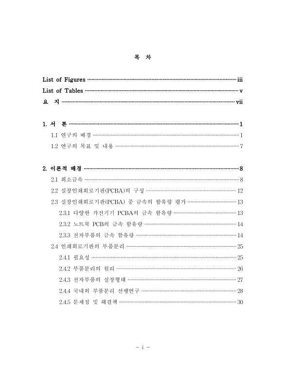
1. 서론 11
1.1. 연구의 배경 11
1.2. 연구의 목표 및 내용 17
2. 이론적 배경 18
2.1. 희소금속 18
2.2. 실장인쇄회로기판(PCBA)의 구성 22
2.3. 실장인쇄회로기판(PCBA) 중 금속의 함유량 평가 23
2.3.1. 다양한 가전기기 PCBA의 금속 함유량 23
2.3.2. 노트북 PCB의 금속 함유량 24
2.3.3. 전자부품의 금속 함유량 24
2.4. 인쇄회로기판의 부품분리 35
2.4.1. 필요성 35
2.4.2. 부품분리의 원리 36
2.4.3. 전자부품의 실장형태 37
2.4.4. 국내외 부품분리 선행연구 38
2.4.5. 문제점 및 해결책 40
3. 부품분리장치 제작 및 실험 방법 45
3.1. 부품분리장비 시작품 45
3.1.1. 부품분리장치의 원리 45
3.1.2. 부품분리장치의 특성 45
3.2. 실험방법 50
3.2.1. 출발원료 50
3.2.2. 부품분리효율 평가 51
3.2.3. 실장형태에 따른 부품분리율 평가 53
3.2.4. 부산물 발생량 평가 53
3.2.5. 부품분리 처리시간 평가 54
4. 결과 및 고찰 56
4.1. 최적조건 도출 56
4.2. 실장형태에 따른 부품분리 특성 평가 61
4.3. 부산물 발생량 평가 65
4.4. 부품분리 처리 시간 평가 66
5. 결론 68
참고문헌 69
ABSTRACT 72
Fig. 1.1. Material involved in metal production. 15
Fig. 1.2. Number of electrical and electronic products in use in households in Korea. 16
Fig. 2.1. Rare metals in the periodic table. 20
Fig. 2.2. Concept of PCBA, PCB and ECs. 22
Fig. 2.3. Metal price of PCB in small electronic appliances. 28
Fig. 2.4. Photograph of PCB. 29
Fig. 2.5. Photograph of CPU/GPU. 30
Fig. 2.6. Photograph of IC chips. 31
Fig. 2.7. Photographs of capacitors. 32
Fig. 2.8. Photograph of slots. 33
Fig. 2.9. Two difference principles of ECs disassembly 42
Fig. 2.10. Previously developed disassembly apparatus 44
Fig. 3.1. Electronic ccmponents disassembly apparatus used in this study 47
Fig. 4.1. Removal efficiency under various conditions 59
Fig. 4.2. Removal efficiency under various feeding rod rtation speed 60
Fig. 4.3. Removal efficiency under various connection types 62
Fig. 4.4. A sample of electronic components before and after the disassembly process under the optimum condition 63
Fig. 4.5. A sample of laptop printed circuit boards before and after the disassembly process under the optimum condition 64
Fig. 4.6. By-product of disassembly processes 65
Fig. 4.7. Disassembly process time 67
*표시는 필수 입력사항입니다.
| 전화번호 |
|---|
| 기사명 | 저자명 | 페이지 | 원문 | 기사목차 |
|---|
| 번호 | 발행일자 | 권호명 | 제본정보 | 자료실 | 원문 | 신청 페이지 |
|---|
도서위치안내: / 서가번호:

우편복사 목록담기를 완료하였습니다.
*표시는 필수 입력사항입니다.
저장 되었습니다.
