
 대표어
대표어

권호기사보기
| 기사명 | 저자명 | 페이지 | 원문 | 기사목차 |
|---|
결과 내 검색
동의어 포함
표제지
목차
국문요약 12
I. 서론 14
1.1. 연구의 배경 및 목적 14
II. 이론적 배경 17
2.1. 비젖음(dewetting)의 이론적 배경 17
2.1.1. 비젖음의 현상학 17
2.1.2. 고상 비젖음 현상의 열역학적 이론 20
2.2. 고상 비젖음(Solid-StateDewetting)의 메커니즘 24
2.2.1. 모세관 현상에 의한 형상 변화 24
2.2.2. 홀(hole)의 생성 27
2.2.3. 홀(hole)의 성장 30
2.3. 단결정 막의 비젖음 40
2.3.1. 형상 기판위의 비젖음 40
2.4. 주기적인 형상기판 위에서의 비젖음 사례 42
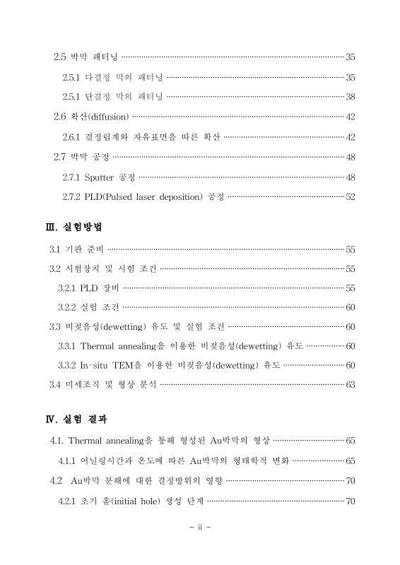
2.5. 박막 패터닝 48
2.5.1. 다결정 막의 패터닝 48
2.5.2. 단결정 막의 패터닝 51
2.6. 확산(diffusion) 55
2.6.1. 결정립계와 자유표면을 따른 확산 55
2.7. 박막 공정 61
2.7.1. Sputter공정 61
2.7.2. PLD(Pulsedlaserdeposition)공정 65
III. 실험방법 68
3.1. 기판 준비 68
3.2. 시험장치 및 시험 조건 68
3.2.1. PLD 장비 68
3.2.2. 실험 조건 73
3.3. 비젖음성(dewetting)유도 및 실험 조건 73
3.3.1. Thermalannealing을 이용한 비젖음성(dewetting)유도 73
3.3.2. In-situTEM을 이용한 비젖음성(dewetting)유도 73
3.4. 미세조직 및 형상 분석 76
IV. 실험 결과 78
4.1. Thermal annealing을 통해 형성된 Au박막의 형상 78
4.1.1. 어닐링시간과 온도에 따른 Au박막의 형태학적 변화 78
4.2. Au박막 분해에 대한 결정방위의 영향 83
4.2.1. 초기 홀(initialhole)생성 단계 83
4.2.2. 각진(facet)홀의 성장 단계 86
4.2.3. 비젖음의 최종 단계 94
4.3. Au박막 분해에 대한 결정립 크기의 영향 98
4.4. Au박막 분해에 대한 결정계의 영향 101
V. 결론 105
참고문헌 107
ABSTRACT 110
Fig 2.1. (a) A measure of the fraction of a glass substrate exposed by dewetting of a Au film (825℃). (b–d) Optical micrographs of... 18
Fig 2.2. (a) Film thickness at which dewetting is observed as a function of annealing temperature for four different metals. (b) Temperature at which dewetting is observed as a function of... 19
Fig 2.3. Schematic illustration of equilibrium film morphology when the equilibrium contact angle θ is nonzero 22
Fig 2.4. Geometric constructions yielding the equilibrium shape of a two-dimensional solid with square symmetry. ■is the surface energy of the solid (film material), ■is the surface...(이미지참조) 23
Fig 2.5. Time evolution of an elongated rectangle with a regular 16-gon equilibrium shape Light gray shapes indicate evolution is motion by surface diffusion and dark gray... 26
Fig 2.6. (a) Schematic cross-sectional view of polycrystalline film with in-plane grain diameter D and radius R on a rigid substrate. (b) The equilibrium shape of polycrystalline film at the... 29
Fig 2.7. Schematic view of the profile of a film edge retracting via surface diffusion 32
Fig 2.8. Schematic profiles of retracting edge according to the (a) Brandon and Bradshaw model, (b) Jiran and Thompson model 33
Fig 2.9. (a) Cross-sectional view of a retracting of a film, after retraction over a distance x0 from the position of the initial edge with a sharp corner. (b-d) As an edge retracts, the rim thickens, and the...(이미지참조) 36
Fig 2.10. A dewetting of 30 nm-thick deposited gold films. 38
Fig 2.11. Schematic illustration of the edge instability that leads to formation of fingerlike morphologies and isolated beads 39
Fig 2.12. Dewetting 120-nm-thick single-crystal Ni films on MgO. (a,b)Atomic force microscopy (AFM) image of holes at an early stage of growth in (a)a(100) film and (b) a(110) film (c,d) AFM images of... 41
Fig 2.13. Schematic illustrations of as-deposited films 45
Fig 2.14. Representative scanning electrin micrographs of the four categories of obseved dewetting on substrates patterned with an array of pits with the shapes of inverted pyramids. Scale bat is 50nm 46
Fig 2.15. An array of crystal direction on topographic template 47
Fig 2.16. SEM images of dewetted 30-nm-thick Au films were (a) initially continuous and (b-d) patterned into different initial shapes. The as-patterned shapes are indicated by the dashed white lines. Scale bars are 5um 49
Fig 2.17. Co nanoparticles formed by thermal annealing and laser annealing 50
Fig 2.18. Single-crystal 120-nm-thick Ni films were patterned into large square patches with edge aligned along different in-plane facets 53
Fig 2.19. Dewetting of square patches patterned from a Ni(110) film. (a)-(d) AFM images of evolving square patches. Scale bars, 4unm. (e)-(h) Height profiles for each of the patterns on the... 54
Fig 2.20. Dewetting of square patches patterned from a Ni(110) film. (a)-(d) AFM images of evolving square patches. Scale bars, 4unm. (e)-(h) Height profiles for each of the patterns on the left. The dashed lines in the height profiles show initial film thickness 58
Fig 2.21. Combined lattice and boundary fluxes during steady-state diffusion through a thin slab of material 59
Fig 2.22. Diffusion in a polycrystalline metal 60
Fig 2.23. Schematic illustration of simple parallel-plate sputtering system 63
Fig 2.24. Plane, cylindricality magnetron sputtering system 64
Fig 2.25. Schematic diagram of vapor deposition concept for PLD 67
Fig 3.1. The image of laser system used in this experiment 69
Fig 3.2. Schematic diagram of laser irradiation 70
Fig 3.3. Rapid heating/cooling system of thermal annealing 74
Fig 3.4. In-situ TEM 75
Fig 3.5. Automated crystallographic orientation and phase mapping system(ASTAR) equipped in the HR-TEM 77
Fig 4.1. Morphological evolution of Au films on silicon nitride substrate during SSD furnace-annealing at 400℃ 80
Fig 4.2. Exposure to heat over time, the fraction of the substrate graph 81
Fig 4.3. Morphological evolution of Au films on silicon nitride substrate during SSD furnace-annealing. 82
Fig 4.4. (a) TEM image showing the voids in the Au film formed during the early stage of dewetting at 400℃, and (b) crystal orientation map of the image 84
Fig 4.5. Illustrate the example of orientation data 85
Fig 4.6. (a) TEM image at an intermediate stage of dewetting at 400℃, and (c) crystal orientation map 87
Fig 4.7. The crystallographic plane of faceted edges represented as numbers as illustrated 88
Fig 4.8. Frequencies of Fig 4.7 as a bar chart 89
Fig 4.9. Production process of Cross-sectional sample at the faceted void edge in FIB 91
Fig 4.10. Cross-sectional TEM images of the faceted boundary at the void edge in the Au film 92
Fig 4.11. Retraction ligaments of the feceted edges of grains 93
Fig 4.12. AFM images of faceted holes of films 95
Fig 4.13. The edge retraction governed by surface diffusion toward top surface of the film 96
Fig 4.14. The crystal orientation mapping for the late stage of dewetting that shows elongated wormlike particles 97
Fig 4.15. TEM images of annealing of the films changed over time at 400℃ 99
Fig 4.16. Grain growth and initial void formation at 400℃ 100
Fig 4.17. Intrusion of initial hole at high angle boundary 102
Fig 4.18. Intrusion of faceted hole at high angle boundary 103
Fig 4.19. The high-resolution images of the corners in faceted grains 104
*표시는 필수 입력사항입니다.
| 전화번호 |
|---|
| 기사명 | 저자명 | 페이지 | 원문 | 기사목차 |
|---|
| 번호 | 발행일자 | 권호명 | 제본정보 | 자료실 | 원문 | 신청 페이지 |
|---|
도서위치안내: / 서가번호:

우편복사 목록담기를 완료하였습니다.
*표시는 필수 입력사항입니다.
저장 되었습니다.
